 |
Labkit Basics
Breadboards
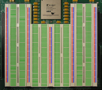
The labkit includes a large breadboard area. This will be useful early in the semester, when you will be working with discrete logic gates, and during the final project, when you may wish to incorporate additional integrated circuits of your own choosing.
The breadboard area is made up of alternating junction blocks and power distribution strips. The holes in the power distribution strips are connected vertically, over the whole height of the breadboard. Holes in the junction blocks are connected horizontally in strips of five. The figure below illustrates this.
To provide power to the distribution strips, jumpers must be run from the strips to the five-position headers located below each distribution strip. The headers provide access to the labkit's ground, 5V, and 3.3V busses. Additionally, +12V and -12V are provided. The 12 volt busses employ linear regulators, for reduced noise. A self-reseting polycrystaline fuse limits the current drawn from each bus to 1A per bus. Should one of the fuses trip, the fuse will reset itself as soon as the load is removed.
Clocks
A 27MHz oscillator is built into the labkit PCB. This oscillator is connected directly to the FPGA, and is accessible via the clock_27mhz signal in the labkit.v file.
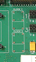
Additionally, two sockets are provided, each of which can accept a full- or half-can oscillator. Any oscillator that can operate at 3.3V can be used. Be careful to install oscillators in the correct orientation: the correct orientation is marked on the board. The outputs of the two oscillator sockets are accessible via the clock1 and clock2 signals in labkit.v.
Switches and Buttons
The labkit includes eight slide switches and nine momentary pushbutton switches. All of the switches are wired directly to the FPGA.
The 8-bit switch signal in the labkit.v file corresponds to the eight slide switches. Each bit of this signal will be a '1' when the corresponding switch is in the up position, and a '0' in the down position.
Four of the pushbuttons are arranged as an up/down/left/right keypad. The remaining buttons are designated "Enter", "0", "1", "2", and "3". The pushbuttons are represented by the signals button_up, button_down, button_left, button_right, button_enter, button0, button1, button2, and button3. The buttons use negative logic, so the above signals are normally '1', and change to '0' when the corresponding buttons are pushed.
Note that none of the switches or buttons are debounced.
LEDs
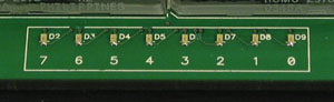
There are eight discrete LEDs on the labkit, which are controlled by the led signal in labkit.v. Writing a "0" to a bit in this signal will turn the corresponding LED on; writing a "1" will turn the LED off.
General-Purpose FPGA I/O
Four banks of 32 signals are provided to
Logic Analyzer Connectors
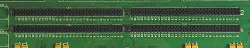
Connectors are provided to interface to four pods of an HP/Agilent logic analyzer. Each pod has 16 data signals and one clock signal.
The clock and data signals to pod 1 are hardwired to the FPGA, and can be accessed via the analyzer1_clock and analyzer1_data signals in labkit.v.
Pods 2-3 are wired to a row of headers near the breadboard area, so that these pods can be used to probe signals from devices on the breadboard.