 |
VGA Video
by Nathan IckesIntroduction
VGA is a high-resolution video standard used mostly for computer monitors, where ability to transmit a sharp, detailed image is essential. VGA uses separate wires to transmit the three color component signals and vertical and horizontal synchronization signals.VGA Signals
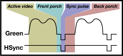
Like any video format, VGA video is a stream of frames: each frame is made up of a series of horizontal lines, and each line is made up of a series of pixels. The lines in each frame are transmitted in order from top to bottom (VGA is not interlaced), and the pixels in each line are transmitted from left to right. Separate horizontal and vertical synchronization signals are used to define the ends of each line and frame. A composite synchronization signal (actually an XOR of the horizontal and vertical signals) is also encoded on the green color channel.
The ADV7125 video DAC reads an 8-bit value for each of the red, green, and blue channels on each cycle of the pixel clock. There is a two-cycle pipeline delay between when the digital codes are read by the DAC and when the corresponding analog voltages appear on the DAC outputs. The RGB input signals can be overridden by the sync and blank signals: The active low blank signal forces all three DAC outputs to their black level, while the active low sync signal forces the green DAC to a special sync level below the normal black level.
Each line of video begins with an active video region, in which RGB values are output for each pixel in the line. The active region is followed by a blanking region, in which black pixels are transmitted. In the middle of the blanking interval, a horizontal sync pulse is transmitted. The blanking interval before the sync pulse is known as the "front porch", and the blanking interval after the sync pulse is known as the "back porch". Note that the dedicated horizontal sync signal output from the FPGA directly to the VGA connector must be delayed by two clock cycles relative to the composite sync signal passed to the DAC chip, to account for the pipeline delay of the DAC.
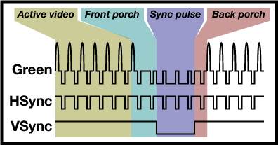
Frames are constructed from lines in much the same way as lines are constructed from pixels. The beginning of a frame contains all of the lines that will actually be displayed on the screen, followed by a number of black lines that make up the front porch. Next comes a vertical sync pulse that lasts for several lines, and then more black lines to make up a back porch. Note that the composite sync signal embedded in the green channel appears inverted during the vertical sync pulse: remember that the composite sync is an XOR of the horizontal and vertical sync signals.
VGA Timings
The following table lists timing values for several popular resolutions.
| Format | Pixel Clock (MHz) |
Horizontal (in Pixels) | Vertical (in Lines) | ||||||
|---|---|---|---|---|---|---|---|---|---|
| Active Video |
Front Porch |
SyncPulse | Back Porch |
Active Video |
Front Porch |
Sync Pulse |
Back Porch |
||
| 640x480, 60Hz | 25.175 | 640 | 16 | 96 | 48 | 480 | 11 | 2 | 31 |
| 640x480, 72Hz | 31.500 | 640 | 24 | 40 | 128 | 480 | 9 | 3 | 28 |
| 640x480, 75Hz | 31.500 | 640 | 16 | 96 | 48 | 480 | 11 | 2 | 32 |
| 640x480, 85Hz | 36.000 | 640 | 32 | 48 | 112 | 480 | 1 | 3 | 25 |
| 800x600, 56Hz | 38.100 | 800 | 32 | 128 | 128 | 600 | 1 | 4 | 14 |
| 800x600, 60Hz | 40.000 | 800 | 40 | 128 | 88 | 600 | 1 | 4 | 23 |
| 800x600, 72Hz | 50.000 | 800 | 56 | 120 | 64 | 600 | 37 | 6 | 23 |
| 800x600, 75Hz | 49.500 | 800 | 16 | 80 | 160 | 600 | 1 | 2 | 21 |
| 800x600, 85Hz | 56.250 | 800 | 32 | 64 | 152 | 600 | 1 | 3 | 27 |
| 1024x768, 60Hz | 65.000 | 1024 | 24 | 136 | 160 | 768 | 3 | 6 | 29 |
| 1024x768, 70Hz | 75.000 | 1024 | 24 | 136 | 144 | 768 | 3 | 6 | 29 |
| 1024x768, 75Hz | 78.750 | 1024 | 16 | 96 | 176 | 768 | 1 | 3 | 28 |
| 1024x768, 85Hz | 94.500 | 1024 | 48 | 96 | 208 | 768 | 1 | 3 | 36 |
As with RS-232, the standard for VGA video is that there are lots of standards. Every manufacturer seems to list different timings in the manuals for their monitors. The values given in the table above are not particularly critical. On a CRT monitor, the lengths of the front and back porches control the position of the image on the display. If the image appears offset to the right or left, or up or down, try adjusting the front and back porch values for the corresponding direction (or use the image position adjustments on the monitor, which accomplish the same thing).
Generating the Pixel Clock
The pixel clock frequency can be synthesized from the 27MHz oscillator built into the labkits by using one of the twelve Digital Clock Managers (DCMs) built into the labkit FPGA. DCMs have numerous uses, one of which is generating a clock signal whose frequency is some multiple of the frequency of a reference clock.
DCMs cannot be inferred by behavioral Verilog: they must be explicitly instantiated. The following Verilog code illustrates how to instantiate a DCM in order to generate a pixel clock.
 DCM pixel_clock_dcm (.CLKIN(clock_27mhz),
                      .CLKFX(pixel_clock));
The reference clock (clock_27mhz in the above example) must be supplied to CLKIN input of the DCM. CLKFX is the frequency-multiplied output clock. The above code fragment leaves many of the DCMs inputs and outputs unconnected: the unconnected ports can safely be ignored in this application.
The operation of a DCM is determined by a number of constraints, which can be entered as special comments in the Verilog code. For our simple frequency synthesis application, only two constraints are essential.
 // synthesis attribute CLKFX_DIVIDE of pixel_clock_dcm is 9
 // synthesis attribute CLKFX_MULTIPLY of pixel_clock_dcm is 26
The CLKFX_MULTIPLY and CLKFX_DIVIDE constraints determine the frequency of the output clock. In the example above, the 27MHz input clock frequency is multiplied by 26 and then divided by 9, resulting in an output frequency of 27*26/9 = 78MHz. CLKFX_MULTIPLY must be between 2 and 32 (inclusive), and CLKFX_DIVIDE must be between 1 and 32.
This has been a very minimal description of how to use a DCM: for a complete explanation of the features and capabilities of DCMs, see the Libraries Guide (PDF) volume of the Xilinx documentation.
More Information
- Datasheet for the ADV7125, Analog Devices.