Course Description
This course covers the theory, design, fabrication and applications of photonic materials and devices. After a survey of optical materials design for semiconductors, dielectrics and polymers, the course examines ray optics, electromagnetic optics and guided wave optics; physics of light-matter interactions; and device …
This course covers the theory, design, fabrication and applications of photonic materials and devices. After a survey of optical materials design for semiconductors, dielectrics and polymers, the course examines ray optics, electromagnetic optics and guided wave optics; physics of light-matter interactions; and device design principles of LEDs, lasers, photodetectors, modulators, fiber and waveguide interconnects, optical filters, and photonic crystals. Device processing topics include crystal growth, substrate engineering, thin film deposition, etching and process integration for dielectric, silicon and compound semiconductor materials. The course also covers microphotonic integrated circuits and applications in telecom/datacom systems. Course assignments include four design projects that emphasize materials, devices and systems applications.
Course Info
Learning Resource Types
grading
Exams
notes
Lecture Notes
assignment
Problem Sets
group_work
Projects

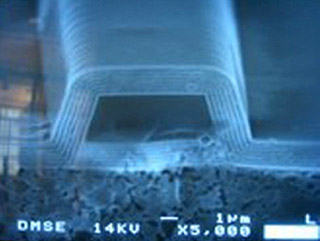
A photonic crystal waveguide manufactured on a silicon wafer using thermal oxidation, UV lithography and Chemical Vapor Deposition at MIT’s Microsystems Technology Laboratories (MTL). See: Yi, Y., S. Akiyama, L. C. Kimerling, et al. Optics Express 12, no. 20 (2004): 4775-4780. (Photo by Prof. Lionel C. Kimerling.)


