
(a) Draw the crystal structure of GaAs, and a separate graphic which is the closest-packed plane and direction on that plane. Discuss the major differences in this structure, as compared to Si.
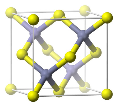
GaAs Zinc-Blende Structure [1]
Image removed due to copyright restrictions.
Please see: http://www-vrl.umich.edu/project2/miller/111plane.JPG
GaAs closest packed direction and plane [2]
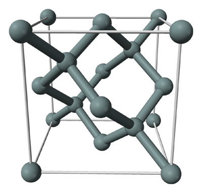
Silicon Diamond Structure [1]
The GaAs structure is a zincblende structure whose basis consists of two different atoms, gallium and arsenic. Silicon has a similar structure except that it has a one atom basis, which is Silicon. This implies the GaAs structure does not have inversion symmetry whereas the silicon structure does. In addition, in GaAs, “the electron clouds [tend] to shift towards the Arsenide atoms, and results in a dipole moment along the [111] axis” [3]; the material exhibits piezoelectric characteristic similar to quartz. The zinc blende structure also offers alternating (111) Gallium and Arsenic planes resulting in very different properties depending on the surface-terminating plane. The asymmetry also results in such properties as hardness, anisotropy, and different dislocation velocities. [3]
(b) From the data provided in Hjort’s Table 1 [3], determine the Poisson’s ratio of GaAs, as compared to Si and AlAs. Discuss comparison of these predictions with experimentally reported values of ν, from open literature and databases such as matweb.com.
Image removed due to copyright restrictions. Please see Table 1 in [3].
The Poisson’s ratio (ν) calculated (by taking the ratio -S12/S11 , values of which are given in table 1) for GaAs, Si, and AlAs are respectively 0.3162, 0.2727, and 0.325. Thus we find that the Poisson’s ratio for AlAs > GaAs > Si. From literature, the Poisson’s ratio for bulk GaAs is 0.31 [4], for Si it ranges between 0.22 for bulk isotropic, and 0.27 for <111> crystalline Si [4], and 0.328 for AlAs [5]. The calculated values are in close agreement with the values got from literature.
(c) Hjort’s Fig. 2 [3] seems to indicate a different number of independent elastic constants than your crystal structure in (a) would suggest; explain. (It’s a simple explanation.)
Image removed due to copyright restrictions. Please see Fig. 2 in [3].
As expected, the matrix in Fig. 2 shows three independent elastic constants, C11, C12 and C44 . However, this matrix has 9x9 elements because it also accounts for the interactions between the mechanical and electromagnetic fields. It displays the relationship between orientation, piezoelectricity, d, and dielectricity, ε and the corresponding responses: SE as the mechanical response to a mechanical force, dT as the mechanical response to an electric field, d as the electrical response to a mechanical force and finally εS as the electrical response to an electrical field.
(d) Based on your analysis of GaAs elastic anisotropy, explain (graphically and/or text) which film orientation you would aim to achieve to create GaAs films or wafers that would be maximally resistant to bending.
Image removed due to copyright restrictions. Please see Fig. 3a in [3].
To resist bending, we want to choose the orientation with the highest Young’s elastic modulus. This is the <111>, as can be seen in Fig. 3a and in our calculations, attached. (PDF)
However, it is important to understand the exact orientation of this the (111) planes with respect to film-substrate interface, which would minimize bending. To do so let us first look at a bi-material strip as shown in the figure below. The two materials can be characterized by different elastic moduli, and thus will exhibit different strains under the same state of stress. This leads to the bending of the strip to incorporate this difference, as understood more clearly by the figure.
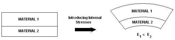
Effect of the introduction of stresses on a bi-material strip.
For a GaAs film on a substrate (of a different material, and thus different elastic modulus, usually much greater), the lattice-mismatch, or a change of environment temperature, etc., generates stresses oriented parallel to the plane of the interface, leading to bending of the thin film, as described above. Also, the elastic modulus of the substrates used, is generally greater than that of the thin film (for example, sapphire, a commonly adopted substrate, has a Young’s Modulus of 400 GPa [6]). Thus, in order to resist bending, it is desired to have the generated stresses experience maximum stiffness. Hence, the (111) planes (greatest modulus) should be oriented such that the normal to these planes are parallel to the generated stresses (in the plane of the interface).
References
[1] Wikimedia Commons.
[3] Hjort, Klas, Jan Soderkvist, and Jan-Ake Schweitz. “Gallium Arsenide as a Mechanical Material.” Journal of Micromechanics and Microengineering 4 (1994): 1-13.
[4] MEMSnet.
[5] Leavitt, R. P., and F. J. Towner. “Determination of the Lattice Parameter and Poisson Ratio for AlAs via High-resolution x-ray-Diffraction Studies of Epitaxial Films.” Physical Review B 48 (1993): 9154-9157.
[6] Moody, N. R., et al. “Substrate Composition Effects on the Interfacial Fracture of Tantalum Nitride Films.” Journal of Materials Research 14 (June 1999): 2306-2313.
Plasticity and fracture of microelectronic thin films/lines
Effects of multidimensional defects on III-V semiconductor mechanics | Problem Set 2 | Problem Set 3 | Problem Set 5
Defect nucleation in crystalline metals
Role of water in accelerated fracture of fiber optic glass
Carbon nanotube mechanics
Superelastic and superplastic alloys
Mechanical behavior of a virus
Effects of radiation on mechanical behavior of crystalline materials


