3-46s06.jpg
Description:
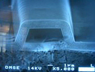
A photonic crystal waveguide manufactured on a silicon wafer using thermal oxidation, UV lithography and chemical vapor deposition at MIT’s Microsystems Technology Laboratories (MTL). See Y. Yi, S. Akiyama, L.C. Kimerling et al., optics express 12 no. 20 (2004):4775-4780. (Photo courtesy of Prof. Lionel C. Kimerling.)
file
19 kB
3-46s06.jpg
Alt text:
Microscope photo of end view of a multi-layered waveguide.
Caption:
A photonic crystal waveguide manufactured on a silicon wafer using thermal oxidation, UV lithography and Chemical Vapor Deposition at MIT’s Microsystems Technology Laboratories (MTL). See: Yi, Y., S. Akiyama, L. C. Kimerling, et al. Optics Express 12, no. 20 (2004): 4775-4780. (Photo by Prof. Lionel C. Kimerling.)

Course Info
Instructors
Departments
As Taught In
Spring
2006
Level
Topics
Learning Resource Types
grading
Exams
notes
Lecture Notes
assignment
Problem Sets
group_work
Projects


