.toc { margin-left: 2em; } .lecslide { margin-top: 1em; margin-bottom: 1em; border-top: 0.5px solid #808080; padding-top: 1em; text-align: center; } .lecslideimg { width: 5in; border: 1px solid black; }
- Our Memory Machine
- Memory Technologies
- Static RAM (SRAM)
- SRAM Cell
- SRAM Read
- SRAM Write
- Multiported SRAMs
- Summary: SRAM
- 1T Dynamic RAM (DRAM) Cell
- 1T DRAM Writes and Reads
- Summary: DRAM
- Non-Volatile Storage: Flash
- Non-Volatile Storage: Hard Disk
- Summary: Memory Technologies
- Memory Hierarchy Interface
- Memory Hierarchy Interface (continued)
- The Locality Principle
- Memory Reference Patterns
- Caches
- A Typical Memory Hierarchy
- Cache Access
- Cache Metrics
- Example: How High of a Hit Ratio?
- Basic Cache Algorithm
- Direct-Mapped Caches
- Example: Direct-Mapped Caches
- Block Size
- Block Size Trandeoffs
- Direct-Mapped Cache Problem: Conflict Misses
- Fully-Associative Cache
- N-way Set-Associative Cache I
- N-way Set-Associative Cache II
- “Let me count the ways.”
- Associativity Tradeoffs
- Associativity Implies Choices
- Replacement Policies
- Write Policy
- Write-Back
- Write-Back with “Dirty” Bits
- Summary: Cache Tradeoffs
Content of the following slides is described in the surrounding text.

In the last lecture we completed the design of the Beta, our reduced-instruction-set computer. The simple organization of the Beta ISA meant that there was a lot commonality in the circuity needed to implement the instructions. The final design has a few main building blocks with MUX steering logic to select input values as appropriate.
If we were to count MOSFETs and think about propagation delays, we’d quickly determine that our 3-port main memory (shown here as the two yellow components) was the most costly component both in terms of space and percentage of the cycle time required by the memory accesses. So in many ways, we really have a “memory machine” instead of a “computing machine”.
The execution of every instruction starts by fetching the instruction from main memory. And ultimately all the data processed by the CPU is loaded from or stored to main memory. A very few frequently-used variable values can be kept in the CPU’s register file, but most interesting programs manipulate *much* more data than can be accommodated by the storage available as part of the CPU datapath.
In fact, the performance of most modern computers is limited by the bandwidth, i.e., bytes/second, of the connection between the CPU and main memory, the so-called memory bottleneck. The goal of this lecture is to understand the nature of the bottleneck and to see if there are architectural improvements we might make to minimize the problem as much as possible.
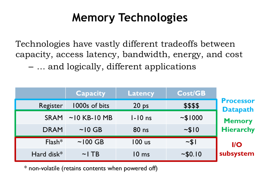
We have a number of memory technologies at our disposal, varying widely in their capacity, latency, bandwidth, energy efficiency and their cost. Not surprisingly, we find that each is useful for different applications in our overall system architecture.
Our registers are built from sequential logic and provide very low latency access (20ps or so) to at most a few thousands of bits of data. Static and dynamic memories, which we’ll discuss further in the coming slides, offer larger capacities at the cost of longer access latencies. Static random-access memories (SRAMs) are designed to provide low latencies (a few nanoseconds at most) to many thousands of locations. Already we see that more locations means longer access latencies — this is a fundamental size vs. performance tradeoff of our current memory architectures. The tradeoff comes about because increasing the number of bits will increase the area needed for the memory circuitry, which will in turn lead to longer signal lines and slower circuit performance due to increased capacitive loads.
Dynamic random-access memories (DRAMs) are optimized for capacity and low cost, sacrificing access latency. As we’ll see in this lecture, we’ll use both SRAMs and DRAMs to build a hybrid memory hierarchy that provides low average latency and high capacity — an attempt to get the best of both worlds!
Notice that the word “average” has snuck into the performance claims. This means that we’ll be relying on statistical properties of memory accesses to achieve our goals of low latency and high capacity. In the worst case, we’ll still be stuck with the capacity limitations of SRAMs and the long latencies of DRAMs, but we’ll work hard to ensure that the worst case occurs infrequently!
Flash memory and hard-disk drives provide non-volatile storage. Non-volatile means that the memory contents are preserved even when the power is turned off. Hard disks are at the bottom of the memory hierarchy, providing massive amounts of long-term storage for very little cost. Flash memories, with a 100-fold improvement in access latency, are often used in concert with hard-disk drives in the same way that SRAMs are used in concert with DRAMs, i.e., to provide a hybrid system for non-volatile storage that has improved latency *and* high capacity.
Let’s learn a bit more about each of these four memory technologies, then we’ll return to the job of building our memory system.
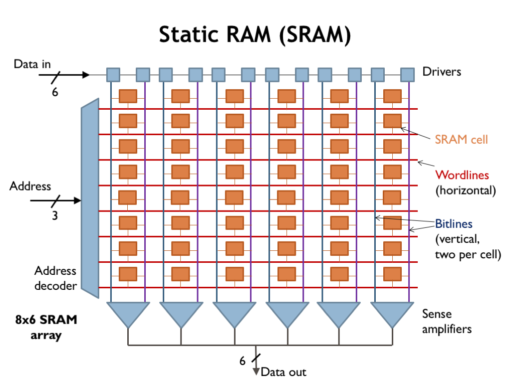
SRAMs are organized as an array of memory locations, where a memory access is either reading or writing all the bits in a single location. Here we see the component layout for a 8-location SRAM array where each location holds 6 bits of data. You can see that the individual bit cells are organized as 8 rows (one row per location) by 6 columns (one column per bit in each memory word). The circuitry around the periphery is used to decode addresses and support read and write operations.
To access the SRAM, we need to provide enough address bits to uniquely specify the location. In this case we need 3 address bits to select one of the 8 memory locations. The address decoder logic sets one of the 8 wordlines (the horizontal wires in the array) high to enable a particular row (location) for the upcoming access. The remaining wordlines are set low, disabling the cells they control. The active wordline enables each of the SRAM bit cells on the selected row, connecting each cell to a pair of bit lines (the vertical wires in the array). During read operations the bit lines carry the analog signals from the enabled bit cells to the sense amplifiers, which convert the analog signals to digital data. During write operations incoming data is driven onto the bit lines to be stored into the enabled bit cells.
Larger SRAMs will have a more complex organization in order to minimize the length, and hence the capacitance, of the bit lines.
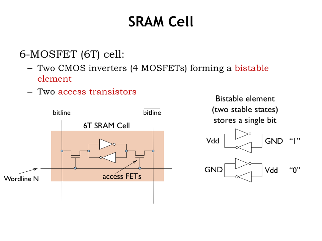
The heart of the SRAM are the bit cells. The typical cell has two CMOS inverters wired in a positive feedback loop to create a bistable storage element. The diagram on the right shows the two stable configurations. In the top configuration, the cell is storing a 1 bit. In the bottom configuration, it’s storing a 0 bit. The cell provides stable storage in the sense that as long as there’s power, the noise immunity of the inverters will ensure that the logic values will be maintained even if there’s electrical noise on either inverter input.
Both sides of the feedback loop are connected via access FETs to the two vertical bit lines. When the wordline connected to the gates of the access FETs is high, the FETs are on, i.e., they will make an electrical connection between the cell’s internal circuity and the bitlines. When the wordline is low, the access FETs are off and the bistable feedback loop is isolated from the bitlines and will happily maintain the stored value as long as there’s power.

During a read operation, the drivers first recharge all the bitlines to Vdd (i.e., a logical 1 value) and then disconnect, leaving the bitlines floating at 1. Then the address decoder sets one of the wordlines high, connecting a row of bit cells to their bitlines. Each cell in the selected row then pulls one of its two bitlines to GND. In this example, it’s the right bitline that’s pulled low. Transitions on the bitlines are slow since the bitline has a large total capacitance and the MOSFETs in the two inverters are small to keep the cell as small as possible. The large capacitance comes partly from the bitline’s length and partly from the diffusion capacitance of the access FETs in other cells in the same column.
Rather than wait for the bitline to reach a valid logic level, sense amplifiers are used to quickly detect the small voltage difference developing between the two bitlines and generate the appropriate digital output. Since detecting small changes in a voltage is very sensitive to electrical noise, the SRAM uses a pair of bitlines for each bit and a differential sense amplifier to provide greater noise immunity.
As you can see, designing a low-latency SRAM involves a lot of expertise with the analog behavior of MOSFETs and some cleverness to ensure electrical noise will not interfere with the correct operation of the circuitry.
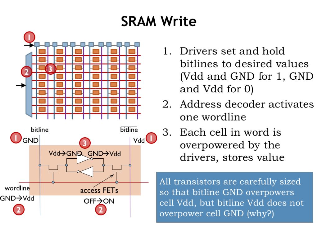
Write operations start by driving the bitlines to the appropriate values. In the example shown here, we want to write a 0-bit into the cell, so the left bitline is set to GND and the right bitline is set to VDD. As before, the address decoder then sets one of the wordlines high, selecting all the cells in a particular row for the write operation.
The drivers have much larger MOSFETs than those in the cell’s inverters, so the internal signals in the enabled cells are forced to the values on the bitlines and the bistable circuits “flip” into the new stable configuration. We’re basically shorting together the outputs of the driver and the internal inverter, so this is another analog operation! This would be a no-no in a strictly digital circuit.
Since n-fets usually carry much higher source-drain currents than p-fets of the same width and given the threshold-drop of the n-fet access transistor, almost all the work of the write is performed by the large n-fet pulldown transistor connected to the bitline with the 0 value, which easily overpowers the small p-fet pullup of the inverters in the cell. Again, SRAM designers need a lot of expertise to correctly balance the sizes of MOSFETs to ensure fast and reliable write operations.
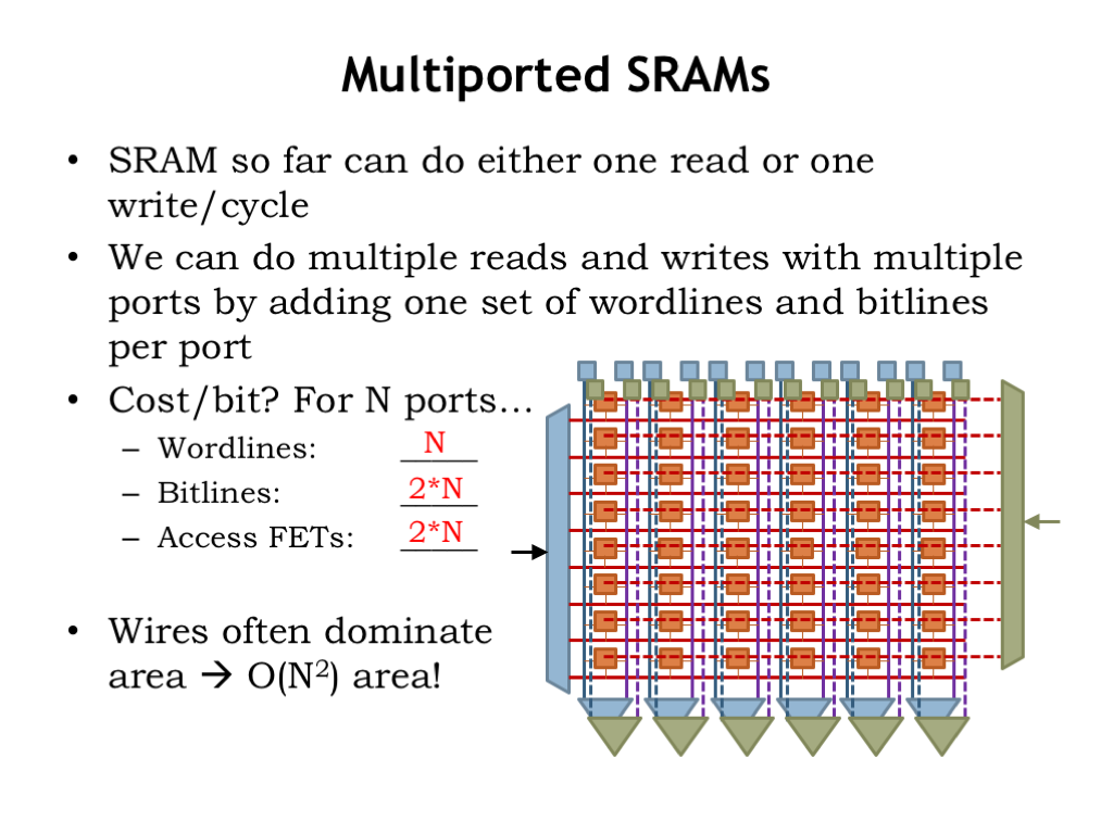
It’s not hard to augment the SRAM to support multiple read/write ports, a handy addition for register file circuits. We’ll do this by adding additional sets of wordlines, bitlines, drivers, and sense amps. This will give us multiple paths to independently access the bistable storage elements in the various rows of the memory array.
With an N-port SRAM, for each bit we’ll need N wordlines, 2N bitlines and 2N access FETs. The additional wordlines increase the effective height of the cell and the additional bitlines increase the effective width of the cell and so the area required by all these wires quickly dominates the size of the SRAM. Since both the height and width of a cell increase when adding ports, the overall area grows as the square of the number of read/write ports. So one has to take care not to gratuitously add ports lest the cost of the SRAM get out of hand.
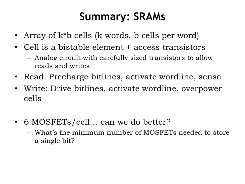
In summary, the circuitry for the SRAM is organized as an array of bit cells, with one row for each memory location and one column for each bit in a location. Each bit is stored by two inverters connected to form a bistable storage element. Reads and writes are essentially analog operations performed via the bitlines and access FETs.
The SRAM uses 6 MOSFETs for each bit cell. Can we do better? What’s the minimum number of MOSFETs needed to store a single bit of information?
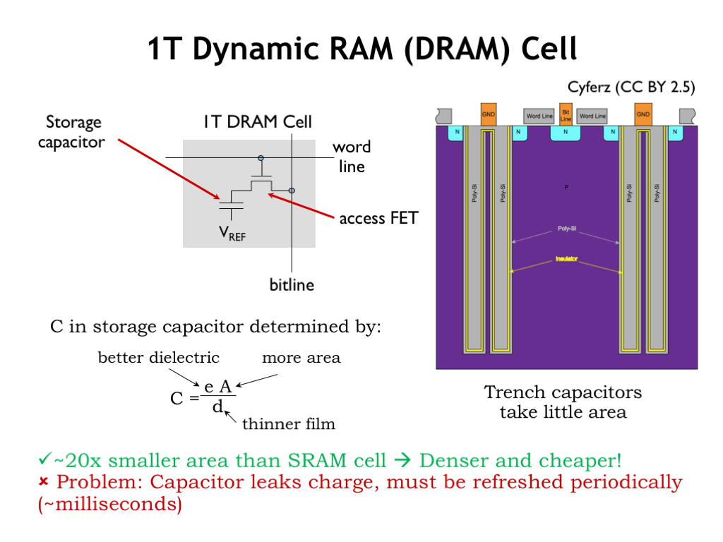
Well, we’ll need at least one MOSFET to serve as the access FET so we can select which bits will be affected by read and write operations. We can use a simple capacitor for storage, where the value of a stored bit is represented by voltage across the plates of the capacitor. The resulting circuit is termed a dynamic random-access memory (DRAM) cell.
If the capacitor voltage exceeds a certain threshold, we’re storing a 1 bit, otherwise we’re storing a 0. The amount of charge on the capacitor, which determines the speed and reliability of reading the stored value, is proportional to the capacitance. We can increase the capacitance by increasing the dielectric constant of the insulating layer between the two plates of the capacitor, increasing the area of the plates, or by decreasing the the distance between the plates. All of these are constantly being improved.
A cross section of a modern DRAM cell is shown here. The capacitor is formed in a large trench dug into the substrate material of the integrated circuit. Increasing the depth of the trench will increase the area of the capacitor plates without increasing the cell’s area. The wordline forms the gate of the N-FET access transistor connecting the outer plate of the capacitor to the bitline. A very thin insulating layer separates the outer plate from the inner plate, which is connected to some reference voltage (shown as GND in this diagram). You can Google trench capacitor to get the latest information on the dimensions and materials used in the construction of the capacitor.
The resulting circuit is quite compact: about 20-times less area/bit than an SRAM bit cell. There are some challenges however. There’s no circuitry to main the static charge on the capacitor, so stored charge will leak from the outer plate of the capacitor, hence the name dynamic memory. The leakage is caused by small picoamp currents through the PN junction with the surrounding substrate, or subthreshold conduction of the access FET even when it’s turned off. This limits the amount of time we can leave the capacitor unattended and still expect to read the stored value. This means we’ll have to arrange to read then re-write each bit cell (called a refresh cycle) every 10ms or so, adding to the complexity of the DRAM interface circuitry.

DRAM write operations are straightforward: simply turn on the access FET with the wordline and charge or discharge the storage capacitor through the bitline.
Reads are bit more complicated. First the bitline is precharged to some intermediate voltage, e.g., VDD/2, and then the precharge circuitry is disconnected. The wordline is activated, connecting the storage capacitor of the selected cell to the bitline causing the charge on the capacitor to be shared with the charge stored by the capacitance of the bitline. If the value stored by the cell capacitor is a 1, the bitline voltage will increase very slightly (e.g., a few tens of millivolts). If the stored value is a 0, the bitline voltage will decrease slightly. Sense amplifiers are used to detect this small voltage change to produce a digital output value.
This means that read operations wipe out the information stored in the bit cell, which must then be rewritten with the detected value at the end of the read operation.
DRAM circuitry is usually organized to have wide rows, i.e., multiple consecutive locations are read in a single access. This particular block of locations is selected by the DRAM row address. Then the DRAM column address is used to select a particular location from the block to be returned. If we want to read multiple locations in a single row, then we only need to send a new column address and the DRAM will respond with that location without having to access the bit cells again. The first access to a row has a long latency, but subsequent accesses to the same row have very low latency. As we’ll see, we’ll be able to use fast column accesses to our advantage.

In summary, DRAM bit cells consist of a single access FET connected to a storage capacitor that’s cleverly constructed to take up as little area as possible. DRAMs must rewrite the contents of bit cells after they are read and every cell must be read and written periodically to ensure that the stored charge is refreshed before it’s corrupted by leakage currents.
DRAMs have much higher capacities than SRAMs because of the small size of the DRAM bit cells, but the complexity of the DRAM interface circuitry means that the initial access to a row of locations is quite a bit slower than an SRAM access. However subsequent accesses to the same row happen at speeds close to that of SRAM accesses.
Both SRAMs and DRAMs will store values as long as their circuitry has power. But if the circuitry is powered down, the stored bits will be lost. For long-term storage we will need to use non-volatile memory technologies, the topic of the next lecture segment.

Non-volatile memories are used to maintain system state even when the system is powered down. In flash memories, long-term storage is achieved by storing charge on an well-insulated conductor called a floating gate, where it will remain stable for years. The floating gate is incorporated in a standard MOSFET, placed between the MOSFET’s gate and the MOSFET’s channel. If there is no charge stored on the floating gate, the MOSFET can be turned on, i.e., be made to conduct, by placing a voltage \(V_1\) on the gate terminal, creating an inversion layer that connects the MOSFET’s source and drain terminals. If there is a charge stored on the floating gate, a higher voltage \(V_2\) is required to turn on the MOSFET. By setting the gate terminal to a voltage between \(V_1\) and \(V_2\), we can determine if the floating gate is charged by testing to see if the MOSFET is conducting.
In fact, if we can measure the current flowing through the MOSFET, we can determine how much charge is stored on the floating gate, making it possible to store multiple bits of information in one flash cell by varying the amount of charge on its floating gate. Flash cells can be connected in parallel or series to form circuits resembling CMOS NOR or NAND gates, allowing for a variety of access architectures suitable for either random or sequential access.
Flash memories are very dense, approaching the areal density of DRAMs, particularly when each cell holds multiple bits of information.
Read access times for NOR flash memories are similar to that of DRAMs, several tens of nanoseconds. Read times for NAND flash memories are much longer, on the order of 10 microseconds. Write times for all types of flash memories are quite long since high voltages have to be used to force electrons to cross the insulating barrier surrounding the floating gate.
Flash memories can only be written some number of times before the insulating layer is damaged to the point that the floating gate will no longer reliably store charge. Currently the number of guaranteed writes varies between 100,000 and 1,000,000. To work around this limitation, flash chips contain clever address mapping algorithms so that writes to the same address actually are mapped to different flash cells on each successive write.
The bottom line is that flash memories are a higher-performance but higher-cost replacement for the hard-disk drive, the long-time technology of choice for non-volatile storage.
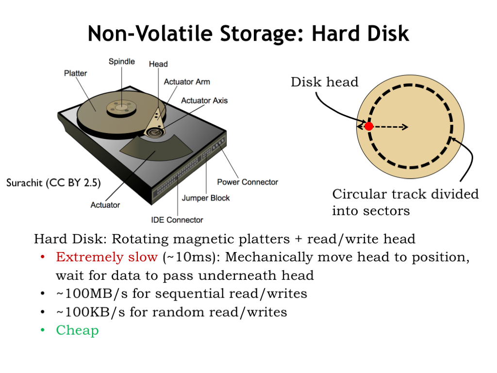
A hard-disk drive (HDD) contains one or more rotating platters coated with a magnetic material. The platters rotate at speeds ranging from 5400 to 15000 RPM. A read/write head positioned above the surface of a platter can detect or change the orientation of the magnetization of the magnetic material below. The read/write head is mounted on an actuator that allows it to be positioned over different circular tracks.
To read a particular sector of data, the head must be positioned radially over the correct track, then wait for the platter to rotate until it’s over the desired sector. The average total time required to correctly position the head is on the order of 10 milliseconds, so hard disk access times are quite long.
However, once the read/write head is in the correct position, data can be transferred at the respectable rate of 100 megabytes/second. If the head has to be repositioned between each access, the effective transfer rate drops 1000-fold, limited by the time it takes to reposition the head.
Hard disk drives provide cost-effective non-volatile storage for terabytes of data, albeit at the cost of slow access times.

This completes our whirlwind tour of memory technologies. If you’d like to learn a bit more, Wikipedia has useful articles on each type of device. SRAM sizes and access times have kept pace with the improvements in the size and speed of integrated circuits. Interestingly, although capacities and transfer rates for DRAMs and HDDs have improved, their initial access times have not improved nearly as rapidly. Thankfully over the past decade flash memories have helped to fill the performance gap between processor speeds and HDDs. But the gap between processor cycle times and DRAM access times has continued to widen, increasing the challenge of designing low-latency high-capacity memory systems.
The capacity of the available memory technologies varies over 10 orders of magnitude, and the variation in latencies varies over 8 orders of magnitude. This creates a considerable challenge in figuring out how to navigate the speed vs size tradeoffs.
Each transition in memory hierarchy shows the same fundamental design choice: we can pick smaller-and-faster or larger-and-slower. This is a bit awkward actually — can we figure how to get the best of both worlds?
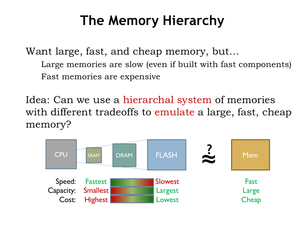
We want our system to behave as if it had a large, fast, and cheap main memory. Clearly we can’t achieve this goal using any single memory technology.
Here’s an idea: can we use a hierarchical system of memories with different tradeoffs to achieve close to the same results as a large, fast, cheap memory? Could we arrange for memory locations we’re using often to be stored, say, in SRAM and have those accesses be low latency? Could the rest of the data could be stored in the larger and slower memory components, moving the between the levels when necessary? Let’s follow this train of thought and see where it leads us.
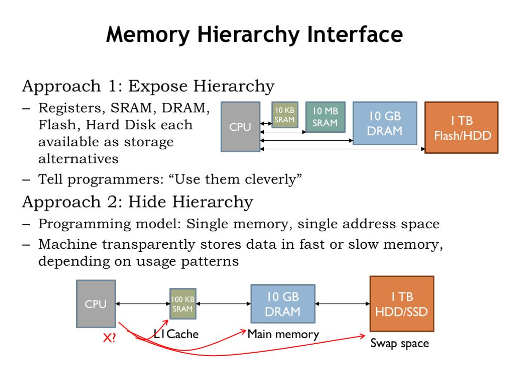
There are two approaches we might take. The first is to expose the hierarchy, providing some amount of each type of storage and let the programmer decide how best to allocate the various memory resources for each particular computation. The programmer would write code that moved data into fast storage when appropriate, then back to the larger and slower memories when low-latency access was no longer required. There would only be a small amount of the fastest memory, so data would be constantly in motion as the focus of the computation changed.
This approach has had notable advocates. Perhaps the most influential was Seymour Cray, the “Steve Jobs” of supercomputers. Cray was the architect of the world’s fastest computers in each of three decades, inventing many of the technologies that form the foundation of high-performance computing. His insight to managing the memory hierarchy was to organize data as vectors and move vectors in and out of fast memory under program control. This was actually a good data abstraction for certain types of scientific computing and his vector machines had the top computing benchmarks for many years.
The second alternative is to hide the hierarchy and simply tell the programmer they have a large, uniform address space to use as they wish. The memory system would, behind the scenes, move data between the various levels of the memory hierarchy, depending on the usage patterns it detected. This would require circuitry to examine each memory access issued by the CPU to determine where in the hierarchy to find the requested location. And then, if a particular region of addresses was frequently accessed — say, when fetching instructions in a loop — the memory system would arrange for those accesses to be mapped to the fastest memory component and automatically move the loop instructions there. All of this machinery would be transparent to the programmer: the program would simply fetch instructions and access data and the memory system would handle the rest.
Could the memory system automatically arrange for the right data to be in the right place at the right time? Cray was deeply skeptical of this approach. He famously quipped “that you can’t fake what you haven’t got”. Wouldn’t the programmer, with her knowledge of how data was going to be used by a particular program, be able to do a better job by explicitly managing the memory hierarchy?
It turns out that when running general-purpose programs, it is possible to build an automatically managed, low-latency, high-capacity hierarchical memory system that appears as one large, uniform memory. What’s the insight that makes this possible? That’s the topic of the next section.
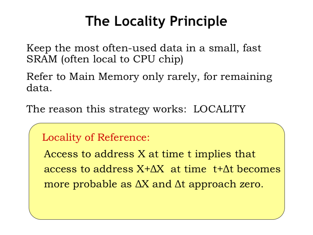
So, how can the memory system arrange for the right data to be in the right place at the right time? Our goal is to have the frequently-used data in some fast SRAM. That means the memory system will have to be able to predict which memory locations will be accessed. And to keep the overhead of moving data into and out of SRAM manageable, we’d like to amortize the cost of the move over many accesses. In other words we want any block of data we move into SRAM to be accessed many times.
When not in SRAM, data would live in the larger, slower DRAM that serves as main memory. If the system is working as planned, DRAM accesses would happen infrequently, e.g., only when it’s time to bring another block of data into SRAM.
If we look at how programs access memory, it turns out we *can* make accurate predictions about which memory locations will be accessed. The guiding principle is locality of reference which tells us that if there’s an access to address X at time t, it’s very probable that the program will access a nearby location in the near future.
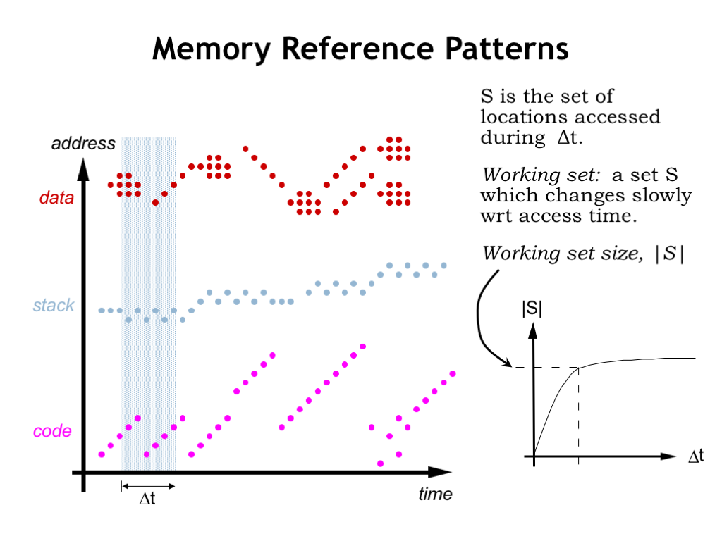
To understand why programs exhibit locality of reference, let’s look at how a running program accesses memory.
Instruction fetches are quite predictable. Execution usually proceeds sequentially since most of the time the next instruction is fetched from the location after that of the current instruction. Code that loops will repeatedly fetch the same sequence of instructions, as shown here on the left of the time line. There will of course be branches and subroutine calls that interrupt sequential execution, but then we’re back to fetching instructions from consecutive locations. Some programming constructs, e.g., method dispatch in object-oriented languages, can produce scattered references to very short code sequences (as shown on the right of the time line) but order is quickly restored.
This agrees with our intuition about program execution. For example, once we execute the first instruction of a procedure, we’ll almost certainly execute the remaining instructions in the procedure. So if we arranged for all the code of a procedure to moved to SRAM when the procedure’s first instruction was fetched, we’d expect that many subsequent instruction fetches could be satisfied by the SRAM. And although fetching the first word of a block from DRAM has relatively long latency, the DRAM’s fast column accesses will quickly stream the remaining words from sequential addresses. This will amortize the cost of the initial access over the whole sequence of transfers.
The story is similar for accesses by a procedure to its arguments and local variables in the current stack frame. Again there will be many accesses to a small region of memory during the span of time we’re executing the procedure’s code.
Data accesses generated by LD and ST instructions also exhibit locality. The program may be accessing the components of an object or struct. Or it may be stepping through the elements of an array. Sometimes information is moved from one array or data object to another, as shown by the data accesses on the right of the timeline.
Using simulations we can estimate the number of different locations that will be accessed over a particular span of time. What we discover when we do this is the notion of a working set of locations that are accessed repeatedly. If we plot the size of the working set as a function of the size of the time interval, we see that the size of the working set levels off. In other words once the time interval reaches a certain size the number of locations accessed is approximately the same independent of when in time the interval occurs.
As we see in our plot to the left, the actual addresses accessed will change, but the number of *different* addresses during the time interval will, on the average, remain relatively constant and, surprisingly, not all that large!
This means that if we can arrange for our SRAM to be large enough to hold the working set of the program, most accesses will be able to be satisfied by the SRAM. We’ll occasionally have to move new data into the SRAM and old data back to DRAM, but the DRAM access will occur less frequently than SRAM accesses. We’ll work out the mathematics in a slide or two, but you can see that thanks to locality of reference we’re on track to build a memory out of a combination of SRAM and DRAM that performs like an SRAM but has the capacity of the DRAM.
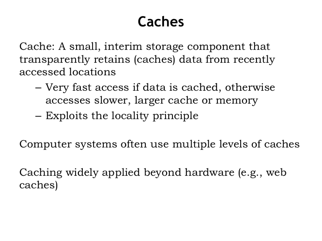
The SRAM component of our hierarchical memory system is called a cache. It provides low-latency access to recently-accessed blocks of data. If the requested data is in the cache, we have a cache hit and the data is supplied by the SRAM.
If the requested data is not in the cache, we have a cache miss and a block of data containing the requested location will have to be moved from DRAM into the cache. The locality principle tells us that we should expect cache hits to occur much more frequently than cache misses.
Modern computer systems often use multiple levels of SRAM caches. The levels closest to the CPU are smaller but very fast, while the levels further away from the CPU are larger and hence slower. A miss at one level of the cache generates an access to the next level, and so on until a DRAM access is needed to satisfy the initial request.
Caching is used in many applications to speed up access to frequently-accessed data. For example, your browser maintains a cache of frequently-accessed web pages and uses its local copy of the web page if it determines the data is still valid, avoiding the delay of transferring the data over the Internet.
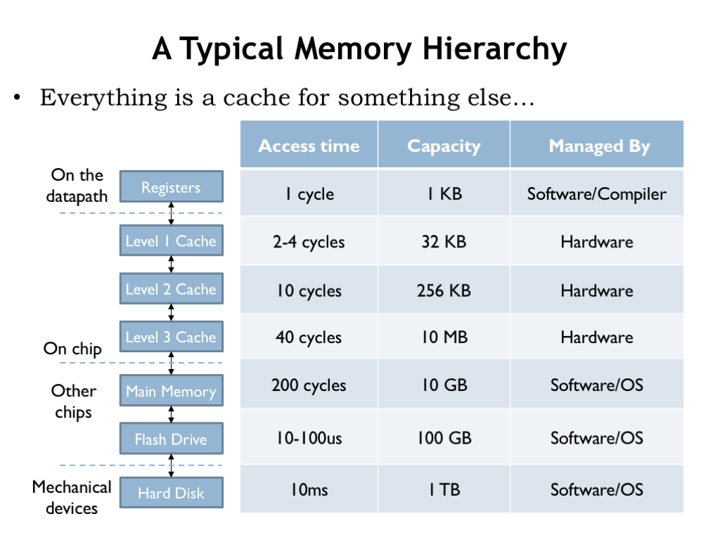
Here’s an example of a memory hierarchy that might be found on a modern computer. There are three levels of on-chip SRAM caches, followed by DRAM main memory and a flash-memory cache for the hard disk drive. The compiler is responsible for deciding which data values are kept in the CPU registers and which values require the use of LDs and STs. The 3-level cache and accesses to DRAM are managed by circuity in the memory system. After that the access times are long enough (many hundreds of instruction times) that the job of managing the movement of data between the lower levels of the hierarchy is turned over to software.
Today we’re discussing how the on-chip caches work. In a later lecture, we’ll discuss how the software manages main memory and non-volatile storage devices. Whether managed by hardware or software, each layer of the memory system is designed to provide lower-latency access to frequently-accessed locations in the next, slower layer. But, as we’ll see, the implementation strategies will be quite different in the slower layers of the hierarchy.
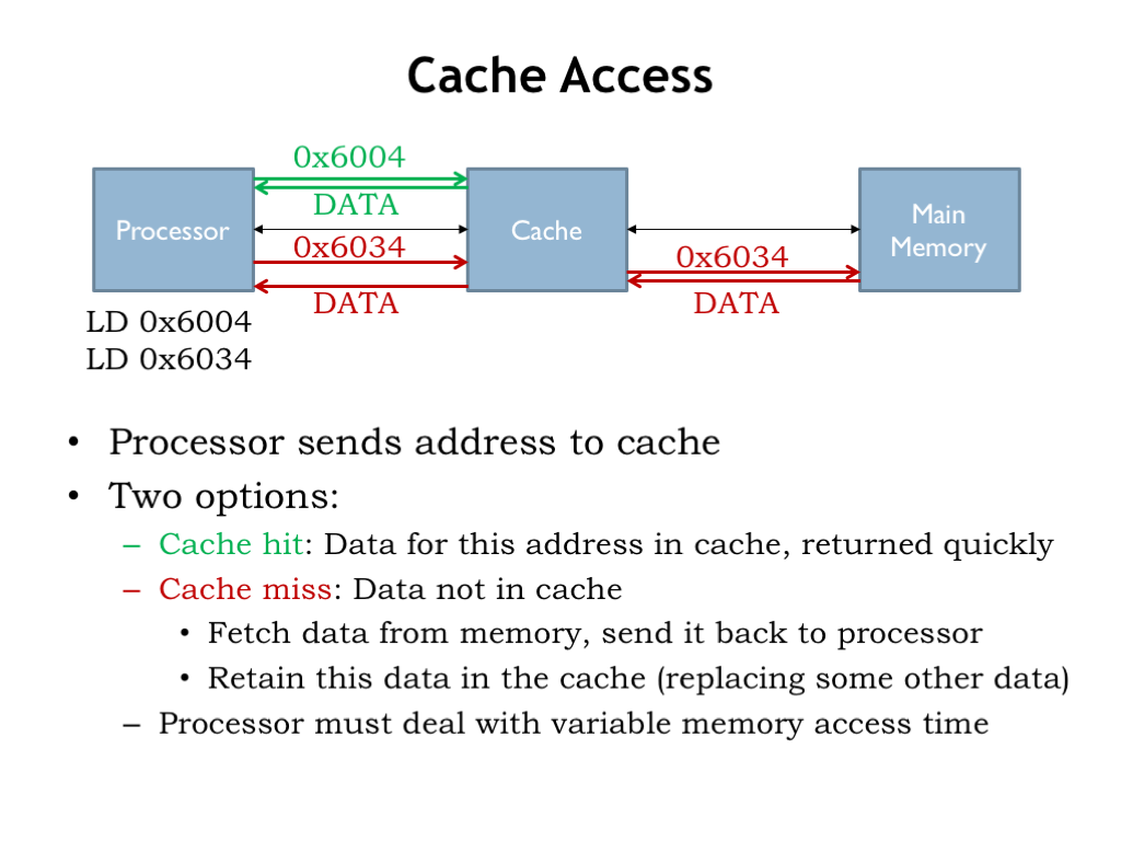
Okay, let’s review our plan. The processor starts an access by sending an address to the cache. If data for the requested address is held in the cache, it’s quickly returned to the CPU.
If the data we request is not in the cache, we have a cache miss, so the cache has to make a request to main memory to get the data, which it then returns to processor. Typically the cache will remember the newly fetched data, possibly replacing some older data in the cache.
Suppose a cache access takes 4 ns and a main memory access takes 40 ns. Then an access that hits in the cache has a latency of 4 ns, but an access that misses in the cache has a latency of 44 ns. The processor has to deal with the variable memory access time, perhaps by simply waiting for the access to complete, or, in modern hyper-threaded processors, it might execute an instruction or two from another programming thread.

The hit and miss ratios tell us the fraction of accesses which are cache hits and the fraction of accesses which are cache misses. Of course, the ratios will sum to 1.
Using these metrics we can compute the average memory access time (AMAT). Since we always check in the cache first, every access includes the cache access time (called the hit time). If we miss in the cache, we have to take the additional time needed to access main memory (called the miss penalty). But the main memory access only happens on some fraction of the accesses: the miss ratio tells us how often that occurs.
So the AMAT can be computed using the formula shown here. The lower the miss ratio (or, equivalently, the higher the hit ratio), the smaller the average access time. Our design goal for the cache is to achieve a high hit ratio.
If we have multiple levels of cache, we can apply the formula recursively to calculate the AMAT at each level of the memory. Each successive level of the cache is slower, i.e., has a longer hit time, which is offset by lower miss ratio because of its increased size.
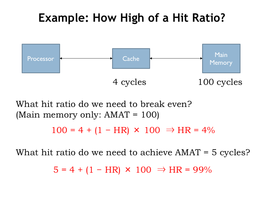
Let’s try out some numbers. Suppose the cache takes 4 processor cycles to respond, and main memory takes 100 cycles. Without the cache, each memory access would take 100 cycles. With the cache, a cache hit takes 4 cycles, and a cache miss takes 104 cycles.
What hit ratio is needed to so that the AMAT with the cache is 100 cycles, the break-even point? Using the AMAT formula from the previously slide, we see that we only need a hit ratio of 4% in order for memory system of the Cache + Main Memory to perform as well as Main Memory alone. The idea, of course, is that we’ll be able to do much better than that.
Suppose we wanted an AMAT of 5 cycles. Clearly most of the accesses would have to be cache hits. We can use the AMAT formula to compute the necessary hit ratio. Working through the arithmetic we see that 99% of the accesses must be cache hits in order to achieve an average access time of 5 cycles.
Could we expect to do that well when running actual programs? Happily, we can come close. In a simulation of the Spec CPU2000 Benchmark, the hit ratio for a standard-size level 1 cache was measured to be 97.5% over some ~10 trillion accesses.
[See the “All benchmarks” arithmetic-mean table at “Cache Performance for SPEC CPU2000 Benchmarks,” Jason F. Cantin and Mark D. Hill.
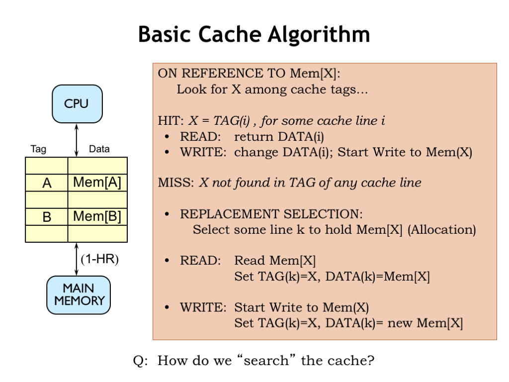
Here’s a start at building a cache. The cache will hold many different blocks of data; for now let’s assume each block is an individual memory location. Each data block is tagged with its address. A combination of a data block and its associated address tag is called a cache line.
When an address is received from the CPU, we’ll search the cache looking for a block with a matching address tag. If we find a matching address tag, we have a cache hit. On a read access, we’ll return the data from the matching cache line. On a write access, we’ll update the data stored in the cache line and, at some point, update the corresponding location in main memory.
If no matching tag is found, we have a cache miss. So we’ll have to choose a cache line to use to hold the requested data, which means that some previously cached location will no longer be found in the cache. For a read operation, we’ll fetch the requested data from main memory, add it to the cache (updating the tag and data fields of the cache line) and, of course, return the data to the CPU. On a write, we’ll update the tag and data in the selected cache line and, at some point, update the corresponding location in main memory.
So the contents of the cache are determined by the memory requests made by the CPU. If the CPU requests a recently-used address, chances are good the data will still be in the cache from the previous access to the same location. As the working set slowly changes, the cache contents will be updated as needed. If the entire working set can fit into the cache, most of the requests will be hits and the AMAT will be close to the cache access time. So far, so good!
Of course, we’ll need to figure how to quickly search the cache, i.e., we’ll a need fast way to answer the question of whether a particular address tag can be found in some cache line. That’s our next topic.
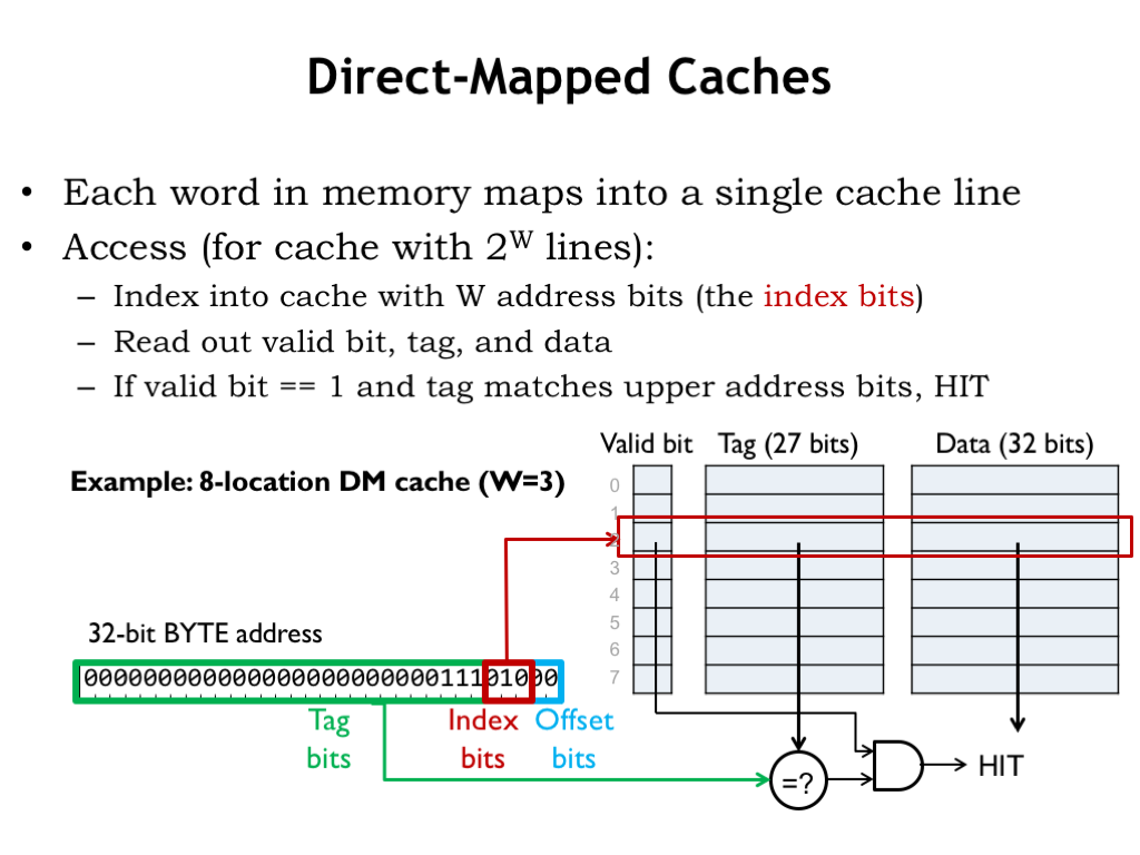
The simplest cache hardware consists of an SRAM with a few additional pieces of logic. The cache hardware is designed so that each memory location in the CPU’s address space maps to a particular cache line, hence the name direct-mapped (DM) cache. There are, of course, many more memory locations then there are cache lines, so many addresses are mapped to the same cache line and the cache will only be able to hold the data for one of those addresses at a time.
The operation of a DM cache is straightforward. We’ll use part of the incoming address as an index to select a single cache line to be searched. The search consists of comparing the rest of the incoming address with the address tag of the selected cache line. If the tag matches the address, there’s a cache hit and we can immediately use the data in the cache to satisfy the request.
In this design, we’ve included an additional valid bit which is 1 when the tag and data fields hold valid information. The valid bit for each cache line is initialized to 0 when the cache is powered on, indicating that all cache lines are empty. As data is brought into the cache, the valid bit is set to 1 when the cache line’s tag and data fields are filled. The CPU can request that the valid bit be cleared for a particular cache line — this is called flushing the cache. If, for example, the CPU initiates a read from disk, the disk hardware will read its data into a block of main memory, so any cached values for that block will be out-of-date. So the CPU will flush those locations from the cache by marking any matching cache lines as invalid.
Let’s see how this works using a small DM cache with 8 lines where each cache line contains a single word (4 bytes) of data. Here’s a CPU request for the location at byte address 0xE8. Since there 4 bytes of data in each cache line, the bottom 2 address bits indicate the appropriate byte offset into the cached word. Since the cache deals only with word accesses, the byte offset bits aren’t used.
Next, we’ll need to use 3 address bits to select which of the 8 cache lines to search. We choose these cache index bits from the low-order bits of the address. Why? Well, it’s because of locality. The principle of locality tells us that it’s likely that the CPU will be requesting nearby addresses and for the cache to perform well, we’d like to arrange for nearby locations to be able to be held in the cache at the same time. This means that nearby locations will have to be mapped to different cache lines. The addresses of nearby locations differ in their low-order address bits, so we’ll use those bits as the cache index bits — that way nearby locations will map to different cache lines.
The data, tag and valid bits selected by the cache line index are read from the SRAM. To complete the search, we check the remaining address against the tag field of the cache. If they’re equal and the valid bit is 1, we have a cache hit, and the data field can be used to satisfy the request.
How come the tag field isn’t 32 bits, since we have a 32-bit address? We could have done that, but since all values stored in cache line 2 will have the same index bits (0b010), we saved a few bits of SRAM and chose not save those bits in the tag. In other words, there’s no point in using SRAM to save bits we can generate from the incoming address.
So the cache hardware in this example is an 8-location by 60 bit SRAM plus a 27-bit comparator and a single AND gate. The cache access time is the access time of the SRAM plus the propagation delays of the comparator and AND gate. About as simple and fast as we could hope for.
The downside of the simplicity is that for each CPU request, we’re only looking in a single cache location to see if the cache holds the desired data. Not much of search is it? But the mapping of addresses to cache lines helps us out here. Using the low-order address bit as the cache index, we’ve arranged for nearby locations to be mapped to different cache lines. So, for example, if the CPU were executing an 8-instruction loop, all 8 instructions can be held in the cache at the same time. A more complicated search mechanism couldn’t improve on that. The bottom line: this extremely simple search is sufficient to get good cache hit ratios for the cases we care about.

Let’s try a few more examples, in this case using a DM cache with 64 lines.
Suppose the cache gets a read request for location 0x400C. To see how the request is processed, we first write the address in binary so we can easily divide it into the offset, index and tag fields. For this address the offset bits have the value 0, the cache line index bits have the value 3, and the tag bits have the value 0x40. So the tag field of cache line 3 is compared with the tag field of the address. Since there’s a match, we have a cache hit and the value in the data field of cache line can be used to satisfy the request.
Would an access to location 0x4008 be a cache hit? This address is similar to that in our first example, except the cache line index is now 2 instead of 3. Looking in cache line 2, we that its tag field (0x58) doesn’t match the tag field in the address (0x40), so this access would be a cache miss.
What are the addresses of the words held by cache lines 0, 1, and 2, all of which have the same tag field? Well, we can run the address matching process backwards! For an address to match these three cache lines it would have look like the binary shown here, where we’ve used the information in the cache tag field to fill in the high-order address bits and low-order address bits will come from the index value. If we fill in the indices 0, 1, and 2, then convert the resulting binary to hex we get 0x5800, 0x5804, and 0x5808 as the addresses for the data held in cache lines 0, 1, and 2.
Note that the complete address of the cached locations is formed by combining the tag field of the cache line with the index of the cache line. We of course need to be able to recover the complete address from the information held in the cache so it can be correctly compared against address requests from the CPU.
We can tweak the design of the DM cache a little to take advantage of locality and save some of the overhead of tag fields and valid bits.
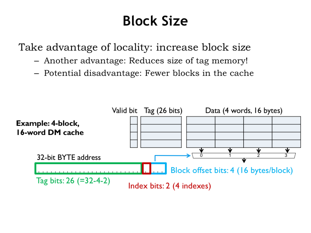
We can increase the size of the data field in a cache from 1 word to 2 words, or 4 words, etc. The number of data words in each cache line is called the block size and is always a power of two. Using a larger block size makes sense. If there’s a high probability of accessing nearby words, why not fetch a larger block of words on a cache miss, trading the increased cost of the miss against the increased probability of future hits.
Compare the 16-word DM cache shown here with a block size of 4 with a different 16-word DM cache with a block size of 1. In this cache for every 128 bits of data there are 27 bits of tags and valid bit, so ~17% of the SRAM bits are overhead in the sense that they’re not being used to store data. In the cache with block size 1, for every 32 bits of data there are 27 bits of tag and valid bit, so ~46% of the SRAM bits are overhead. So a larger block size means we’ll be using the SRAM more efficiently.
Since there are 16 bytes of data in each cache line, there are now 4 offset bits. The cache uses the high-order two bits of the offset to select which of the 4 words to return to the CPU on a cache hit.
There are 4 cache lines, so we’ll need two cache line index bits from the incoming address.
And, finally, the remaining 26 address bits are used as the tag field.
Note that there’s only a single valid bit for each cache line, so either the entire 4-word block is present in the cache or it’s not. Would it be worth the extra complication to support caching partial blocks? Probably not. Locality tells us that we’ll probably want those other words in the near future, so having them in the cache will likely improve the hit ratio.
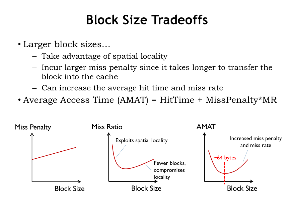
What’s the tradeoff between block size and performance? We’ve argued that increasing the block size from 1 was a good idea. Is there a limit to how large blocks should be? Let’s look at the costs and benefits of an increased block size.
With a larger block size we have to fetch more words on a cache miss and the miss penalty grows linearly with increasing block size. Note that since the access time for the first word from DRAM is quite high, the increased miss penalty isn’t as painful as it might be.
Increasing the block size past 1 reduces the miss ratio since we’re bringing words into the cache that will then be cache hits on subsequent accesses. Assuming we don’t increase the overall cache capacity, increasing the block size means we’ll make a corresponding reduction in the number of cache lines. Reducing the number of lines impacts the number of separate address blocks that can be accommodated in the cache. As we saw in the discussion on the size of the working set of a running program, there are a certain number of separate regions we need to accommodate to achieve a high hit ratio: program, stack, data, etc. So we need to ensure there are a sufficient number of blocks to hold the different addresses in the working set. The bottom line is that there is an optimum block size that minimizes the miss ratio and increasing the block size past that point will be counterproductive.
Combining the information in these two graphs, we can use the formula for AMAT to choose the block size the gives us the best possible AMAT. In modern processors, a common block size is 64 bytes (16 words).
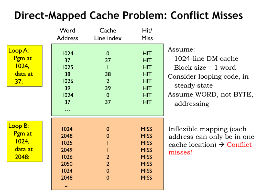
DM caches do have an Achilles heel. Consider running the 3-instruction LOOPA code with the instructions located starting at word address 1024 and the data starting at word address 37 where the program is making alternating accesses to instruction and data, e.g., a loop of LD instructions.
Assuming a 1024-line DM cache with a block size of 1, the steady state hit ratio will be 100% once all six locations have been loaded into the cache since each location is mapped to a different cache line.
Now consider the execution of the same program, but this time the data has been relocated to start at word address 2048. Now the instructions and data are competing for use of the same cache lines. For example, the first instruction (at address 1024) and the first data word (at address 2048) both map to cache line 0, so only one them can be in the cache at a time. So fetching the first instruction fills cache line 0 with the contents of location 1024, but then the first data access misses and then refills cache line 0 with the contents of location 2048. The data address is said to conflict with the instruction address. The next time through the loop, the first instruction will no longer be in the cache and its fetch will cause a cache miss, called a conflict miss. So in the steady state, the cache will never contain the word requested by the CPU.
This is very unfortunate! We were hoping to design a memory system that offered the simple abstraction of a flat, uniform address space. But in this example we see that simply changing a few addresses results in the cache hit ratio dropping from 100% to 0%. The programmer will certainly notice her program running 10 times slower!
So while we like the simplicity of DM caches, we’ll need to make some architectural changes to avoid the performance problems caused by conflict misses.
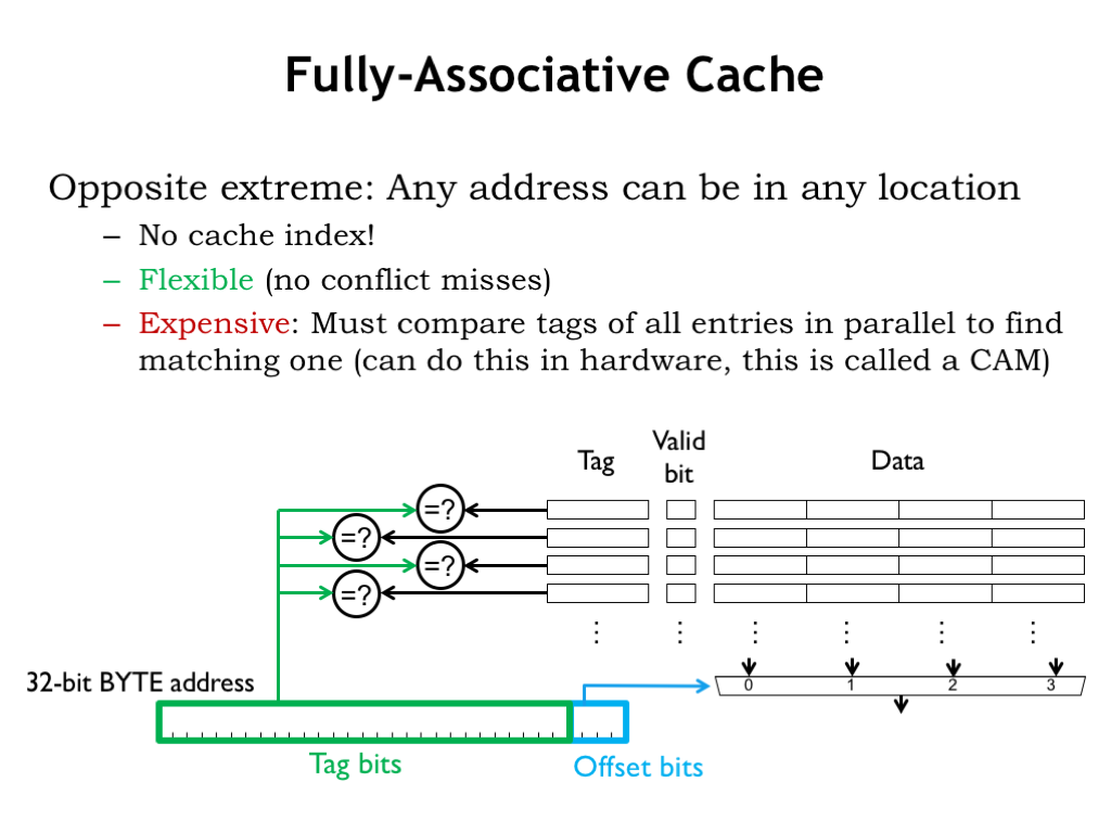
A fully-associative (FA) cache has a tag comparator for each cache line. So the tag field of *every* cache line in a FA cache is compared with the tag field of the incoming address. Since all cache lines are searched, a particular memory location can be held in any cache line, which eliminates the problems of address conflicts causing conflict misses. The cache shown here can hold 4 different 4-word blocks, regardless of their address. The example from the end of the previous segment required a cache that could hold two 3-word blocks, one for the instructions in the loop, and one for the data words. This FA cache would use two of its cache lines to perform that task and achieve a 100% hit ratio regardless of the addresses of the instruction and data blocks.
FA caches are very flexible and have high hit ratios for most applications. Their only downside is cost: the inclusion of a tag comparator for each cache line to implement the parallel search for a tag match adds substantially the amount of circuitry required when there are many cache lines. Even the use of hybrid storage/comparison circuitry, called a content-addressable memory, doesn’t make a big dent in the overall cost of a FA cache.
DM caches searched only a single cache line. FA caches search all cache lines. Is there a happy middle ground where some small number of cache lines are searched in parallel?
Yes! If you look closely at the diagram of the FA cache shown here, you’ll see it looks like four 1-line DM caches operating in parallel. What would happen if we designed a cache with four multi-line DM caches operating in parallel?
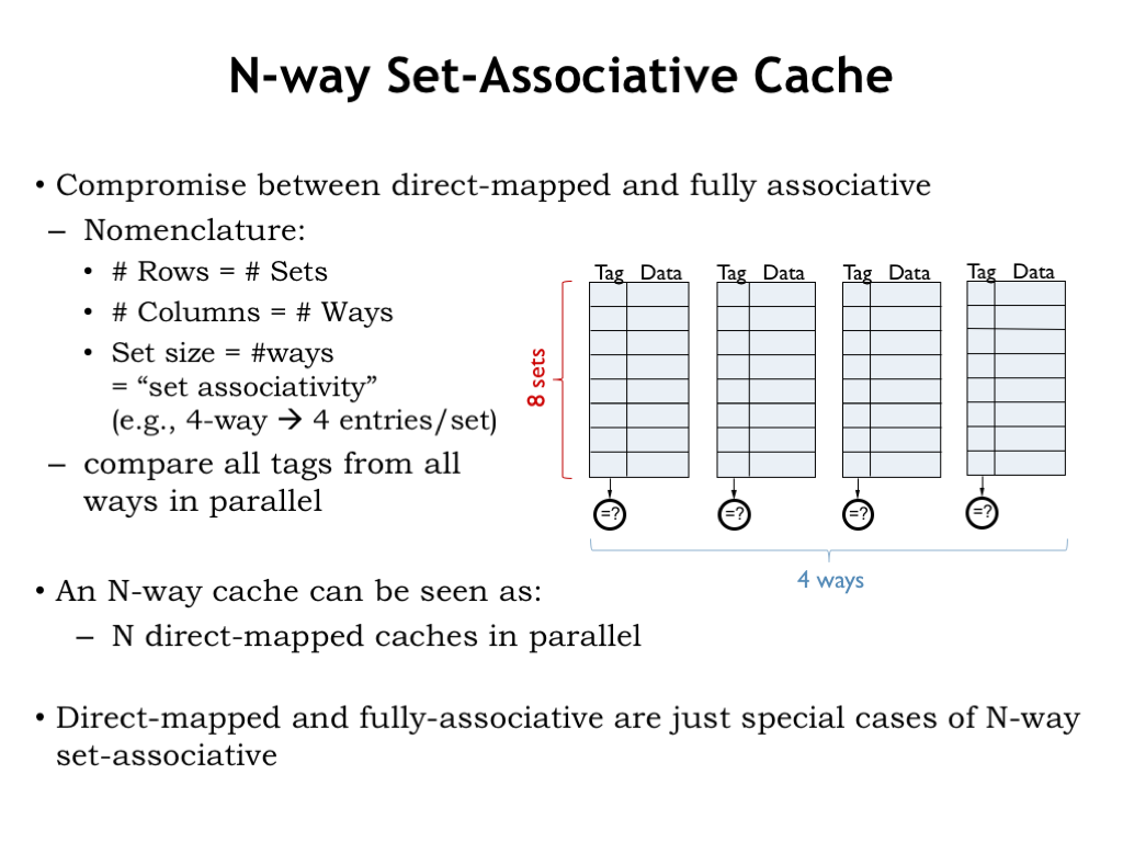
The result would be what we call an 4-way set-associative (SA) cache. An N-way SA cache is really just N DM caches (let’s call them sub-caches) operating in parallel. Each of the N sub-caches compares the tag field of the incoming address with the tag field of the cache line selected by the index bits of the incoming address. The N cache lines searched on a particular request form a search set and the desired location might be held in any member of the set.
The 4-way SA cache shown here has 8 cache lines in each sub-cache, so each set contains 4 cache lines (one from each sub-cache) and there are a total of 8 sets (one for each line of the sub-caches).
An N-way SA cache can accommodate up to N blocks whose addresses map to the same cache index. So access to up to N blocks with conflicting addresses can still be accommodated in this cache without misses. This a big improvement over a DM cache where an address conflict will cause the current resident of a cache line to be evicted in favor of the new request.
And an N-way SA cache can have a very large number of cache lines but still only have to pay the cost of N tag comparators. This is a big improvement over a FA cache where a large number of cache lines would require a large number of comparators.
So N-way SA caches are a good compromise between a conflict-prone DM cache and the flexible but very expensive FA cache.
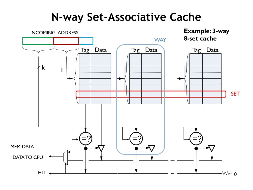
Here’s a slightly more detailed diagram, in this case of a 3-way 8-set cache. Note that there’s no constraint that the number of ways be a power of two since we aren’t using any address bits to select a particular way. This means the cache designer can fine tune the cache capacity to fit her space budget.
Just to review the terminology: the N cache lines that will be searched for a particular cache index are called a set. And each of N sub-caches is called a way.
The hit logic in each way operates in parallel with the logic in other ways. Is it possible for a particular address to be matched by more than one way? That possibility isn’t ruled out by the hardware, but the SA cache is managed so that doesn’t happen. Assuming we write the data fetched from DRAM during a cache miss into a single sub-cache - we’ll talk about how to choose that way in a minute — there’s no possibility that more than one sub-cache will ever match an incoming address.
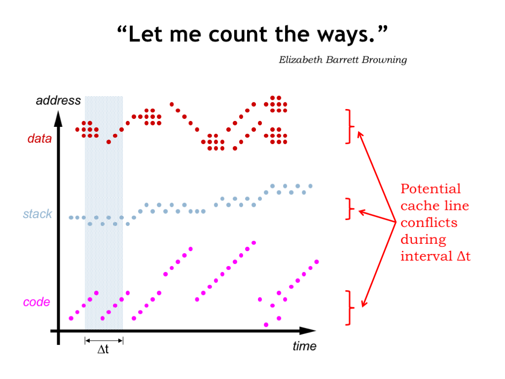
How many ways to do we need? We’d like enough ways to avoid the cache line conflicts we experienced with the DM cache. Looking at the graph we saw earlier of memory accesses vs. time, we see that in any time interval there are only so many potential address conflicts that we need to worry about.
The mapping from addresses to cache lines is designed to avoid conflicts between neighboring locations. So we only need to worry about conflicts between the different regions: code, stack and data. In the examples shown here there are three such regions, maybe 4 if you need two data regions to support copying from one data region to another. If the time interval is particularly large, we might need double that number to avoid conflicts between accesses early in the time interval and accesses late in the time interval.
The point is that a small number of ways should be sufficient to avoid most cache line conflicts in the cache.

As with block size, it’s possible to have too much of a good thing: there’s an optimum number of ways that minimizes the AMAT. Beyond that point, the additional circuity needed to combine the hit signals from a large number of ways will start have a significant propagation delay of its own, adding directly to the cache hit time and the AMAT.
More to the point, the chart on the left shows that there’s little additional impact on the miss ratio beyond 4 to 8 ways. For most programs, an 8-way set-associative cache with a large number of sets will perform on a par with the much more-expensive FA cache of equivalent capacity.
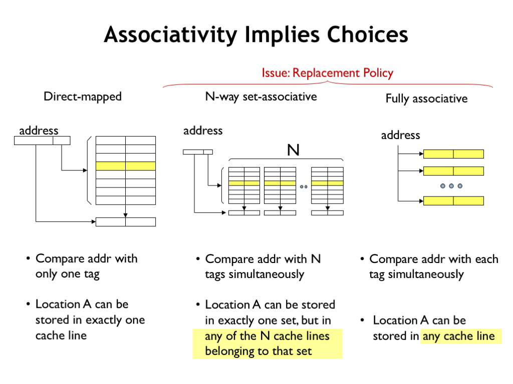
There’s one final issue to resolve with SA and FA caches. When there’s a cache miss, which cache line should be chosen to hold the data that will be fetched from main memory? That’s not an issue with DM caches, since each data block can only be held in one particular cache line, determined by its address. But in N-way SA caches, there are N possible cache lines to choose from, one in each of the ways. And in a FA cache, any of the cache lines can be chosen.
So, how to choose? Our goal is to choose to replace the contents of the cache line which will minimize the impact on the hit ratio in the future.
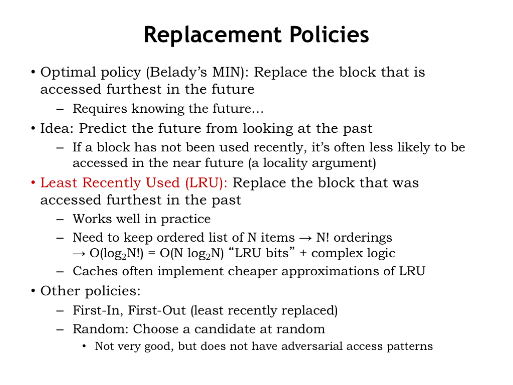
The optimal choice is to replace the block that is accessed furthest in the future (or perhaps is never accessed again). But that requires knowing the future…
Here’s an idea: let’s predict future accesses by looking at recent accesses and applying the principle of locality. If a block has not been recently accessed, it’s less likely to be accessed in the near future.
That suggests the least-recently-used replacement strategy, usually referred to as LRU: replace the block that was accessed furthest in the past. LRU works well in practice, but requires us to keep a list ordered by last use for each set of cache lines, which would need to be updated on each cache access. When we needed to choose which member of a set to replace, we’d choose the last cache line on this list. For an 8-way SA cache there are 8! possible orderings, so we’d need log2(8!) = 16 state bits to encode the current ordering. The logic to update these state bits on each access isn’t cheap; basically you need a lookup table to map the current 16-bit value to the next 16-bit value. So most caches implement an approximation to LRU where the update function is much simpler to compute.
There are other possible replacement policies: First-in, first-out, where the oldest cache line is replaced regardless of when it was last accessed. And Random, where some sort of pseudo-random number generator is used to select the replacement.
All replacement strategies except for random can be defeated. If you know a cache’s replacement strategy you can design a program that will have an abysmal hit rate by accessing addresses you know the cache just replaced. I’m not sure I care about how well a program designed to get bad performance runs on my system, but the point is that most replacement strategies will occasionally cause a particular program to execute much more slowly than expected.
When all is said and done, an LRU replacement strategy or a close approximation is a reasonable choice.
Okay, one more cache design decision to make, then we’re done!
How should we handle memory writes in the cache? Ultimately we’ll need update main memory with the new data, but when should that happen?
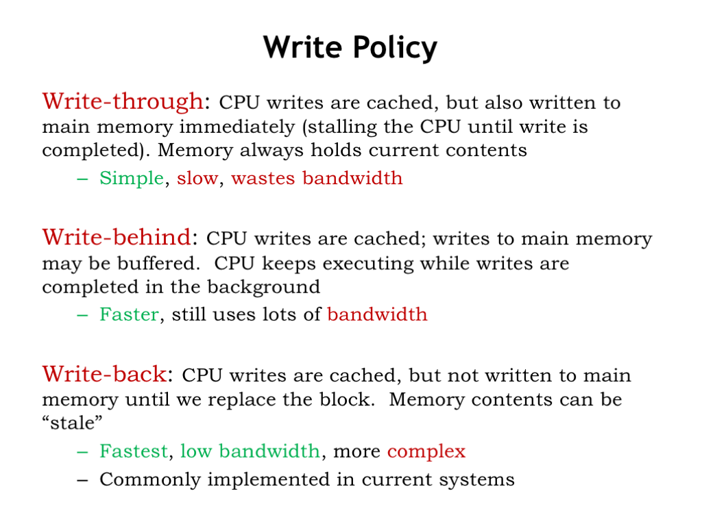
The most obvious choice is to perform the write immediately. In other words, whenever the CPU sends a write request to the cache, the cache then performs the same write to main memory. This is called write-through. That way main memory always has the most up-to-date value for all locations. But this can be slow if the CPU has to wait for a DRAM write access — writes could become a real bottleneck! And what if the program is constantly writing a particular memory location, e.g., updating the value of a local variable in the current stack frame? In the end we only need to write the last value to main memory. Writing all the earlier values is waste of memory bandwidth.
Suppose we let the CPU continue execution while the cache waits for the write to main memory to complete — this is called write-behind. This will overlap execution of the program with the slow writes to main memory. Of course, if there’s another cache miss while the write is still pending, everything will have to wait at that point until both the write and subsequent refill read finish, since the CPU can’t proceed until the cache miss is resolved.
The best strategy is called write-back where the contents of the cache are updated and the CPU continues execution immediately. The updated cache value is only written to main memory when the cache line is chosen as the replacement line for a cache miss. This strategy minimizes the number of accesses to main memory, preserving the memory bandwidth for other operations. This is the strategy used by most modern processors.

Write-back is easy to implement. Returning to our original cache recipe, we simply eliminate the start of the write to main memory when there’s a write request to the cache. We just update the cache contents and leave it at that.
However, replacing a cache line becomes a more complex operation, since we can’t reuse the cache line without first writing its contents back to main memory in case they had been modified by an earlier write access.
Hmm. Seems like this does a write-back of all replaced cache lines whether or not they’ve been written to.
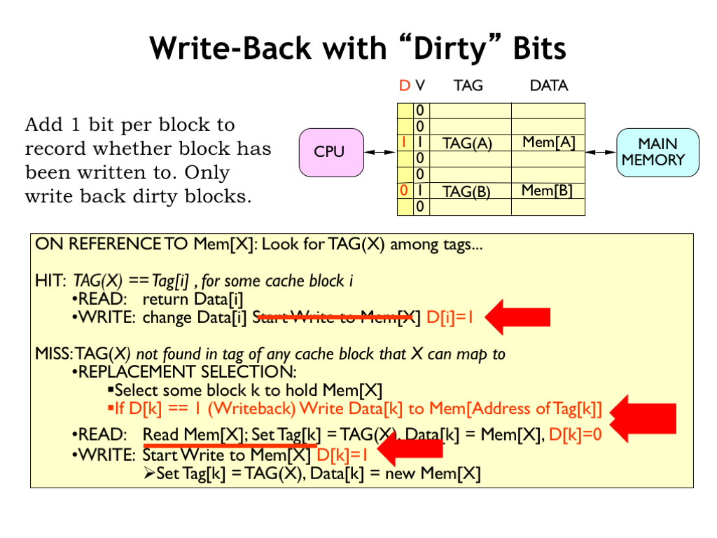
We can avoid unnecessary write-backs by adding another state bit to each cache line: the dirty bit. The dirty bit is set to 0 when a cache line is filled during a cache miss. If a subsequent write operation changes the data in a cache line, the dirty bit is set to 1, indicating that value in the cache now differs from the value in main memory.
When a cache line is selected for replacement, we only need to write its data back to main memory if its dirty bit is 1.
So a write-back strategy with a dirty bit gives an elegant solution that minimizes the number of writes to main memory and only delays the CPU on a cache miss if a dirty cache line needs to be written back to memory.

That concludes our discussion of caches, which was motivated by our desire to minimize the average memory access time by building a hierarchical memory system that had both low latency and high capacity.
There were a number of strategies we employed to achieve our goal.
Increasing the number of cache lines decreases AMAT by decreasing the miss ratio.
Increasing the block size of the cache let us take advantage of the fast column accesses in a DRAM to efficiently load a whole block of data on a cache miss. The expectation was that this would improve AMAT by increasing the number of hits in the future as accesses were made to nearby locations.
Increasing the number of ways in the cache reduced the possibility of cache line conflicts, lowering the miss ratio.
Choosing the least-recently used cache line for replacement minimized the impact of replacement on the hit ratio.
And, finally, we chose to handle writes using a write-back strategy with dirty bits.
How do we make the tradeoffs among all these architectural choices? As usual, we’ll simulate different cache organizations and chose the architectural mix that provides the best performance on our benchmark programs.


