L13: Building the Beta
- CPU Design Tradeoffs
- Processor Performance
- Reminder: Beta ISA
- Approach: Incremental Featurism
- Multi-ported Register File
- Register File Timing
- ALU Instructions
- Instruction Fetch/Decode
- ALU Op Datapath I
- ALU Op Datapath II
- ALU Operations (with constant) I
- ALU Operations (with constant) II
- Load Instruction I
- Load Instruction II
- Store Instruction I
- Store Instruction II
- JMP Instruction I
- JMP Instruction II
- BEQ/BNE Instructions I
- BEQ/BNE Instructions II
- Load Relative Instruction
- LDR Instruction I
- LDR Instruction II
- Exceptions
- Exception Processing
- Exception Implementation
- Exceptions I
- Exceptions II
- Beta: Our “Final Answer”
- Control Logic
- Beta Inside!
Content of the following slides is described in the surrounding text.
Today we’re going to describe the datapath and control logic needed to execute Beta instructions. In an upcoming lab assignment, we’ll ask you to build a working implementation using our standard cell library. When you’re done, you’ll have designed and debugged a 32-bit reduced-instruction set computer! Not bad…
Before tackling a design task, it’s useful to understand the goals for the design. Functionality, of course; in our case the correct execution of instructions from the Beta ISA. But there are other goals we should think about.
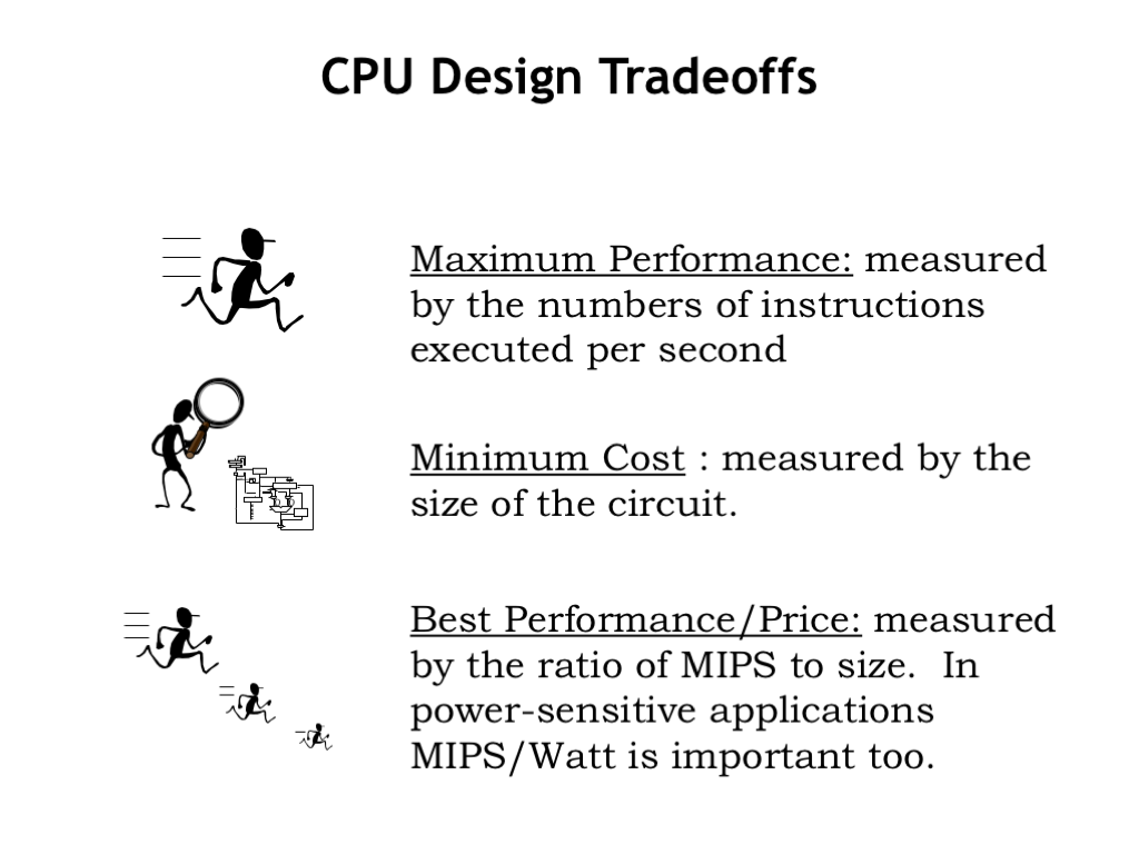
An obvious goal is to maximize performance, as measured by the number of instructions executed per second. This is usually expressed in MIPS, an acronym for “Millions of Instructions Per Second”. When the Intel 8080 was introduced in 1974, it executed instructions at 0.29 MIPS or 290,000 instructions per second as measured by the Dhrystone benchmark. Modern multi-core processors are rated between 10,000 and 100,000 MIPS.
Another goal might be to minimize the manufacturing cost, which in integrated circuit manufacturing is proportional to the size of the circuit.
Or we might want have the best performance for a given price. In our increasingly mobile world, the best performance per watt might be an important goal.
One of the interesting challenges in computer engineering is deciding exactly how to balance performance against cost and power efficiency. Clearly the designers of the Apple Watch have a different set of design goals then the designers of high-end desktop computers.
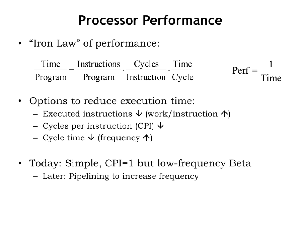
The performance of a processor is inversely proportional to the length of time it takes to run a program. The shorter the execution time, the higher the performance. The execution time is determined by three factors.
First, the number of instructions in the program.
Second, the number of clock cycles our sequential circuit requires to execute a particular instruction. Complex instructions, e.g., adding two values from main memory, may make a program shorter, but may also require many clock cycles to perform the necessary memory and datapath operations.
Third, the amount of time needed for each clock cycle, as determined by the propagation delay of the digital logic in the datapath.
So to increase the performance we could reduce the number of instructions to be executed. Or we can try to minimize the number of clock cycles needed on the average to execute our instructions. There’s obviously a bit of a tradeoff between these first two options: more computation per instruction usually means it will take more time to execute the instruction. Or we can try to keep our logic simple, minimizing its propagation delay in the hopes of having a short clock period.
Today we’ll focus on an implementation for the Beta ISA that executes one instruction every clock cycle. The combinational paths in our circuit will be fairly long, but, as we learned in Part 1 of the course, this gives us the opportunity to use pipelining to increase our implementation’s throughput. We’ll talk about the implementation of a pipelined processor in some upcoming lectures.

Here’s a quick refresher on the Beta ISA. The Beta has thirty-two 32-bit registers that hold values for use by the datapath. The first class of ALU instructions, which have 0b10 as the top 2 bits of the opcode field, perform an operation on two register operands (Ra and Rb), storing the result back into a specified destination register (Rc). There’s a 6-bit opcode field to specify the operation and three 5-bit register fields to specify the registers to use as source and destination. The second class of ALU instructions, which have 0b11 in the top 2 bits of the opcode, perform the same set of operations where the second operand is constant in the range -32768 to +32767.
The operations include arithmetic operations, comparisons, boolean operations, and shifts. In assembly language, we use a “C” suffix added to the mnemonics shown here to indicate that the second operand is a constant.
This second instruction format is also used by the instructions that access memory and change the normally sequential execution order.
The use of just two instruction formats will make it very easy to build the logic responsible for translating the encoded instructions into the signals needed to control the operation of the datapath. In fact, we’ll be able to use many of the instruction bits as-is!

We’ll build our datapath incrementally, starting with the logic needed to perform the ALU instructions, then add additional logic to execute the memory and branch instructions. Finally, we’ll need to add logic to handle what happens when an exception occurs and execution has to be suspended because the current instruction cannot be executed correctly.
We’ll be using the digital logic gates we learned about in Part 1 of the course. In particular, we’ll need multi-bit registers to hold state information from one instruction to the next. Recall that these memory elements load new values at the rising edge of the clock signal, then store that value until the next rising clock edge.
We’ll use a lot of multiplexers in our design to select between alternative values in the datapath.
The actual computations will be performed by the arithmetic and logic unit (ALU) that we designed at the end of Part 1. It has logic to perform the arithmetic, comparison, boolean and shift operations listed on the previous slide. It takes in two 32-bit operands and produces a 32-bit result.
And, finally, we’ll use several different memory components to implement register storage in the datapath and also for main memory, where instructions and data are stored.
You might find it useful to review the chapters on combinational and sequential logic in Part 1 of the course.
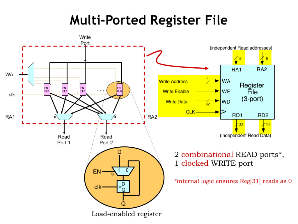
The Beta ISA specifies thirty-two 32-bit registers as part of the datapath. These are shown as the magenta rectangles in the diagram above. These are implemented as load-enabled registers, which have an EN signal that controls when the register is loaded with a new value. If EN is 1, the register will be loaded from the D input at the next rising clock edge. If EN is 0, the register is reloaded with its current value and hence its value is unchanged. It might seem easier to add enabling logic to the clock signal, but this is almost never a good idea since any glitches in that logic might generate false edges that would cause the register to load a new value at the wrong time. Always remember the mantra: NO GATED CLOCKS!
There are multiplexers (shown underneath the registers) that let us select a value from any of the 32 registers. Since we need two operands for the datapath logic, there are two such multiplexers. Their select inputs (RA1 and RA2) function as addresses, determining which register values will be selected as operands. And, finally, there’s a decoder that determines which of the 32 register load enables will be 1 based on the 5-bit WA input.
For convenience, we’ll package all this functionality up into a single component called a “register file”. The register file has two read ports, which given a 5-bit address input, deliver the selected register value on the read-data ports. The two read ports operate independently. They can read from different registers or, if the addresses are the same, read from the same register.
The signals on the left of the register file include a 5-bit value (WA) that selects a register to be written with the specified 32-bit write data (WD). If the write enable signal (WE) is 1 at the rising edge of the clock (CLK) signal, the selected register will be loaded with the supplied write data.
Note that in the BETA ISA, reading from register address 31 should always produce a zero value. The register file has internal logic to ensure that happens.
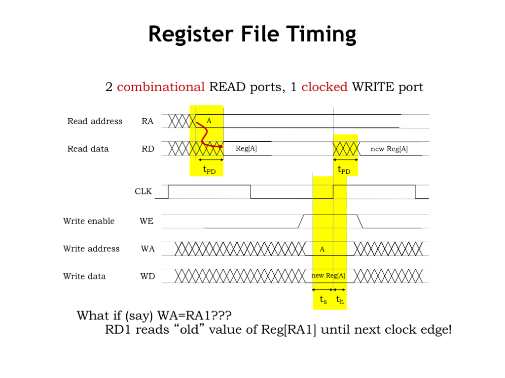
Here’s a timing diagram that shows the register file in operation. To read a value from the register file, supply a stable address input (RA) on one of read ports. After the register file’s propagation delay, the value of the selected register will appear on the corresponding read data port (RD).
Not surprisingly, the register file write operation is very similar to writing an ordinary D-register. The write address (WA), write data (WD) and write enable (WE) signals must all be valid and stable for some specified setup time before the rising edge of the clock. And must remain stable and valid for the specified hold time after the rising clock edge. If those timing constraints are met, the register file will reliably update the value of the selected register.
When a register value is written at the rising clock edge, if that value is selected by a read address, the new data will appear after the propagation delay on the corresponding data port. In other words, the read data value changes if either the read address changes or the value of the selected register changes.
Can we read and write the same register in a single clock cycle? Yes! If the read address becomes valid at the beginning of the cycle, the old value of the register will be appear on the data port for the rest of the cycle. Then, the write occurs at the *end* of the cycle and the new register value will be available in the next clock cycle.
Okay, that’s a brief run-though of the components we’ll be using. Let’s get started on the design!

Our first task is to work on the datapath logic needed to execute ALU instructions with two register operands. Each instruction requires the same processing steps:
Fetch, where the 32-bit encoded instruction is read from main memory from the location specified by the program counter (PC).
Decode, where the opcode field (instruction bits [31:26]) is used to determine the values for the datapath control signals.
Read, where the contents of the registers specified by the RA and RB fields (instruction bits [20:16] and [15:11]) are read from the register file.
Execute, where the requested operation is performed on the two operand values. We’ll also need to compute the next value for the PC.
And Write-back, where the result of the operation is written to the register file in the register specified by the RC field (instruction bits [25:21]).
The system’s clock signal is connected to the register file and the PC register. At the rising edge of the clock, the new values computed during the Execute phase are written to these registers. The rising clock edge thus marks the end of execution for the current instruction and the beginning of execution for the next instruction. The period of the clock, i.e., the time between rising clock edges, needs to be long enough to accommodate the cumulative propagation delay of the logic that implements the 5 steps described here. Since one instruction is executed each clock cycle, the frequency of the clock tells us the rate at which instructions are executed. If the clock period was 10ns, the clock frequency would be 100 MHz and our Beta would be executing instructions at 100 MIPS!
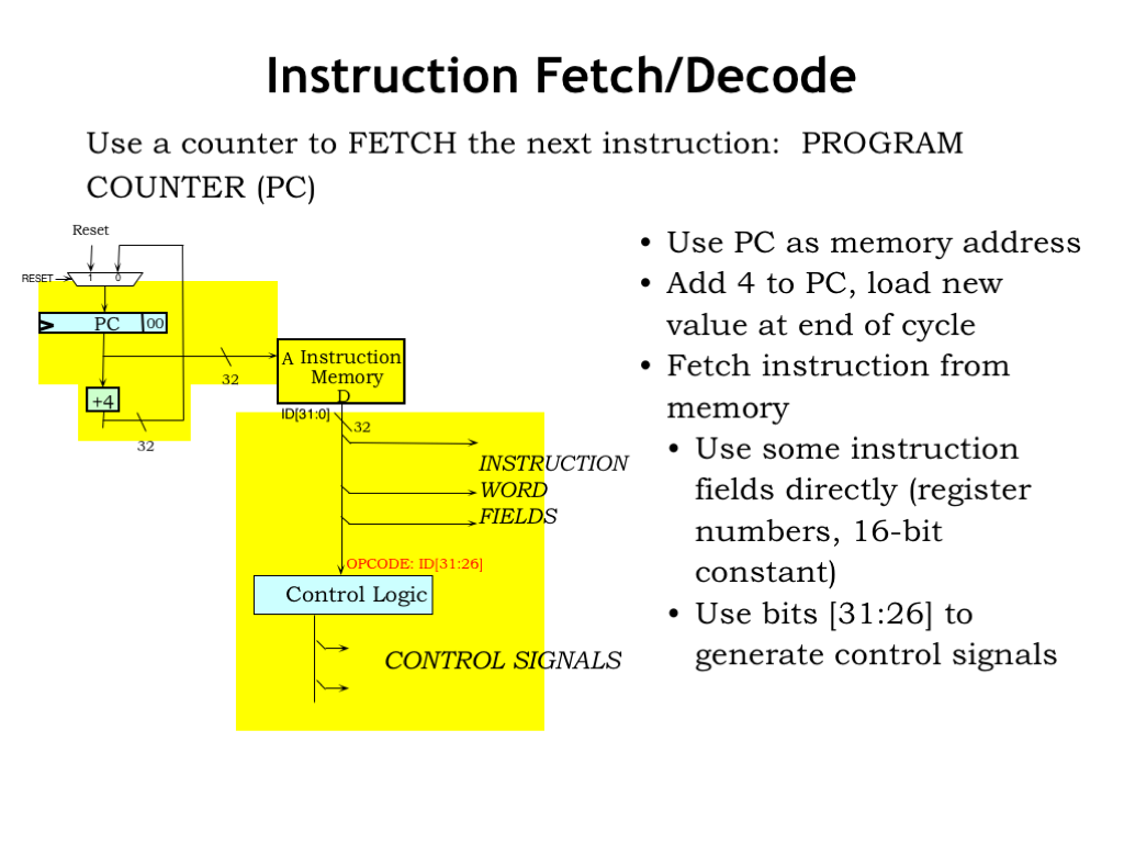
Here’s a sketch showing the hardware needed for the Fetch and Decode steps.
The current value of the PC register is routed to main memory as the address of the instruction to be fetched.
For ALU instructions, the address of the next instruction is simply the address of the current instruction plus 4. There’s an adder dedicated to performing the “PC+4” computation and that value is routed back to be used as the next value of the PC. We’ve also included a MUX used to select the initial value for the PC when the RESET signal is 1.
After the memory propagation delay, the instruction bits (ID[31:0]) are available and the processing steps can begin. Some of the instruction fields can be used directly as-is. To determine the values for other control signals, we’ll need some logic that computes their values from the bits of the opcode field.

Now let’s fill in the datapath logic needed to execute ALU instructions with two register operands. The instruction bits for the 5-bit RA, RB and RC fields can be connected directly to the appropriate address inputs of the register file. The RA and RB fields supply the addresses for the two read ports and the RC field supplies the address for the write port.
The outputs of the read data ports are routed to the inputs of the ALU to serve as the two operands. The ALUFN control signals tell the ALU what operation to perform. These control signals are determined by control logic from the 6-bit opcode field. For specificity, let’s assume that the control logic is implemented using a read-only memory (ROM), where the opcode bits are used as the ROM’s address and the ROM’s outputs are the control signals. Since there are 6 opcode bits, we’ll need \(2^6 = 64\) locations in the ROM. We’ll program the contents of the ROM to supply the correct control signal values for each of the 64 possible opcodes.
The output of the ALU is routed back to the write data port of the register file, to be written into the RC register at the end of the cycle. We’ll need another control signal, WERF (“write-enable register file”), that should have the value 1 when we want to write into the RC register. Let me introduce you to Werf, the 6.004 mascot, who, of course, is named after her favorite control signal, which she’s constantly mentioning.
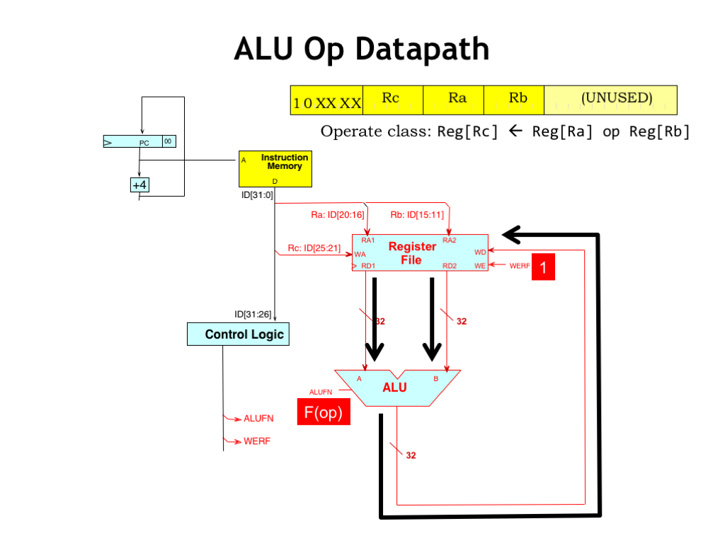
Let’s follow the flow of data as we execute the ALU instruction. After the instruction has been fetched, supplying the RA and RB instruction fields, the RA and RB register values appear on the read data ports of the register file.
The control logic has decoded the opcode bits and supplied the appropriate ALU function code. You can find a listing of the possible function codes in the upper right-hand corner of the Beta Diagram handout.
The result of the ALU’s computation is sent back to the register file to be written into the RC register. Of course, we’ll need to set WERF to 1 to enable the write.
Here we see one of the major advantages of a reduced-instruction set computer architecture: the datapath logic required for execution is very straightforward!

The other form of ALU instructions uses a constant as the second ALU operand. The 32-bit operand is formed by sign-extending the 16-bit two’s complement constant stored in the literal field (bits [15:0]) of the instruction. In order to select the sign-extended constant as the second operand, we added a MUX to the datapath. When its BSEL control signal is 0, the output of the register file is selected as the operand. When BSEL is 1, the sign-extended constant is selected as the operand. The rest of the datapath logic is the same as before.
Note that no logic gates are needed to perform sign-extension — it’s all done with wiring! To sign-extend a two’s complement number, we just need to replicate the high-order, or sign, bit as many times as necessary. You might find it useful to review the discussion of two’s complement in Lecture 1 of Part 1 of the course. So to form a 32-bit operand from a 16-bit constant, we just replicate its high-order bit (ID[15]) sixteen times as we make the connection to the BSEL MUX.
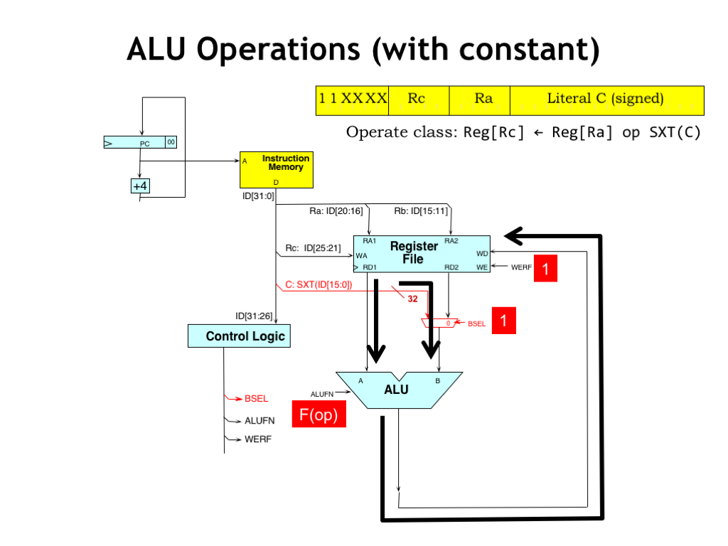
During execution of ALU-with-constant instructions, the flow of data is much as it was before. The one difference is that the control logic sets the BSEL control signal to 1, selecting the sign-extended constant as the second ALU operand.
As before, the control logic generates the appropriate ALU function code and the output of the ALU is routed to the register file to be written back to the RC register.
Amazingly, this datapath is sufficient to execute most of the instructions in the Beta ISA! We just have the memory and branch instruction left to implement. That’s our next task.

The LD and ST instructions access main memory. Note that it’s the same main memory that holds the instructions, even though for drafting convenience we show it as two separate boxes in our datapath diagram. In the form we show it here, main memory has three ports: two read ports for fetching instructions and reading load data, and one write port used by the ST instruction to write data into main memory.
The address calculation is exactly the same computation as performed by the ADDC instruction: the contents of the RA register are added to the sign-extended 16-bit literal from the low-order 16 bits of the instruction. So we’ll simply reuse the existing datapath hardware to compute the address.
For the LD instruction the output of the ALU is routed to main memory as the address of the location we wish to access. After the memory’s propagation delay, the contents of the addressed location is returned by the memory and we need to route that back to the register file to be written into the RC register.
The memory has two control signals: MOE (memory output enable), which we set to 1 when we want to read a value from the memory. And MWE (memory write enable) which is set to 1 when we want main memory to store the value on its write data (WD) port into the addressed memory location.
We need to add another MUX to select which value to write back to the register file: the output of the ALU or the data returning from main memory. We’ve used a 3-to-1 MUX and we’ll see the use for the other MUX input when we get to the implementation of branches and jumps. The two-bit WDSEL signal is used to select the source of the write-back value.

Let’s follow the flow of data when executing the LD instruction. The ALU operands are chosen just as they are for the ADDC instruction and the ALU is requested to perform an ADD operation.
The ALU result is connected to the address port of main memory, whose control signals are set for a read operation. The WDSEL control signals are set to 2 to route the returning data to the register file.
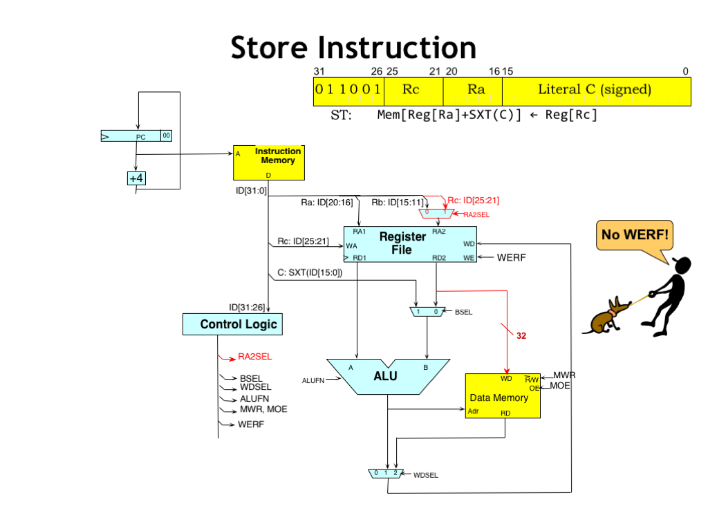
Execution of the ST instruction is very similar to the execution of the LD instruction, with one extra complication. The value to be written to memory comes from the RC register, but the RC instruction field is not connected a register file read address.
Happily, the RB register address isn’t being used by the ST instruction since the second ALU operand comes from the literal field. So we’ll use a MUX to enable the RC field to be selected as the address for the register file’s second read port. When the RA2SEL control signal is 0, the RB field is selected as the address. When RA2SEL is 1, the RC field is selected.
The output from the second read data port is connected to the write data port of main memory.
The ST instruction is the only instruction that does not write a result into the register file. So the WERF control signal will be 0 when executing ST.
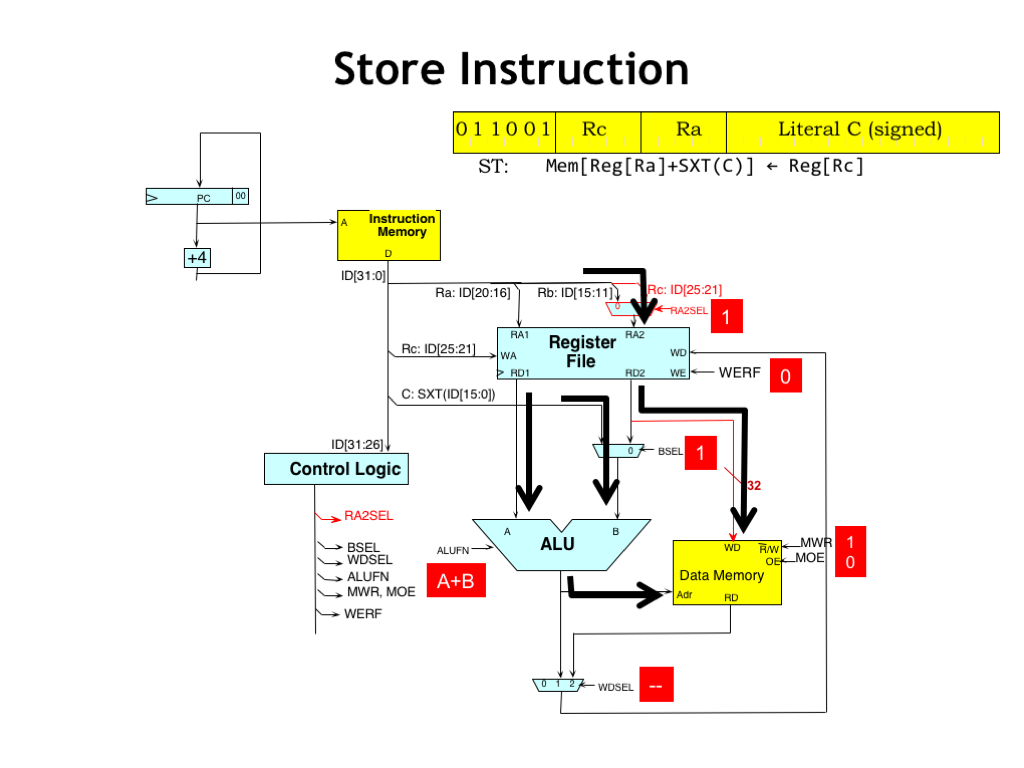
Here’s the flow of data when executing ST. The operands are selected as for LD and the ALU performs the address computation with the result sent to main memory as the address.
Meanwhile the RC field is selected as the address for the second register file read port and the value from the RC register becomes the write data for main memory. By setting the MWR control signal to 1, the main memory will write the WD data into the selected memory location at the end of the cycle.
The WERF control signal is set to zero since we won’t be writing a value into the register file. And, since we’re not writing to the register file, we don’t care about the value for the WDSEL signal.
Of course, the logic will need to supply some value for WDSEL. The “don’t care” annotation is telling the logic designer that she’s welcome to supply whatever value is most convenient. This is particularly useful when using Karnaugh maps to optimize the control logic, where the value can be chosen as either 0 or 1, whichever results in the best minimization of the logic equations.
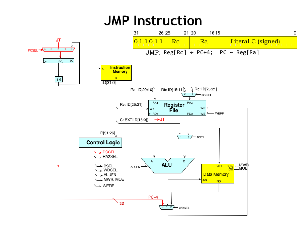
We’re on the home stretch now. For all the instructions up until now, the next instruction has come from the location following the current instruction — hence the “PC+4” logic. Branches and JMPs change that by altering the value in the PC.
The JMP instruction simply takes the value in the RA register and makes it the next PC value. The PCSEL MUX in the upper left-hand corner lets the control logic select the source of the next PC value. When PCSEL is 0, the incremented PC value is chosen. When PCSEL is 2, the value of the RA register is chosen. We’ll see how the other inputs to the PCSEL MUX are used in just a moment.
The JMP and branch instructions also cause the address of the following instruction, i.e., the PC+4 value, to be written to the RC register. When WDSEL is 0, the “0” input of the WDSEL MUX is used to select the PC+4 value as the write-back data.
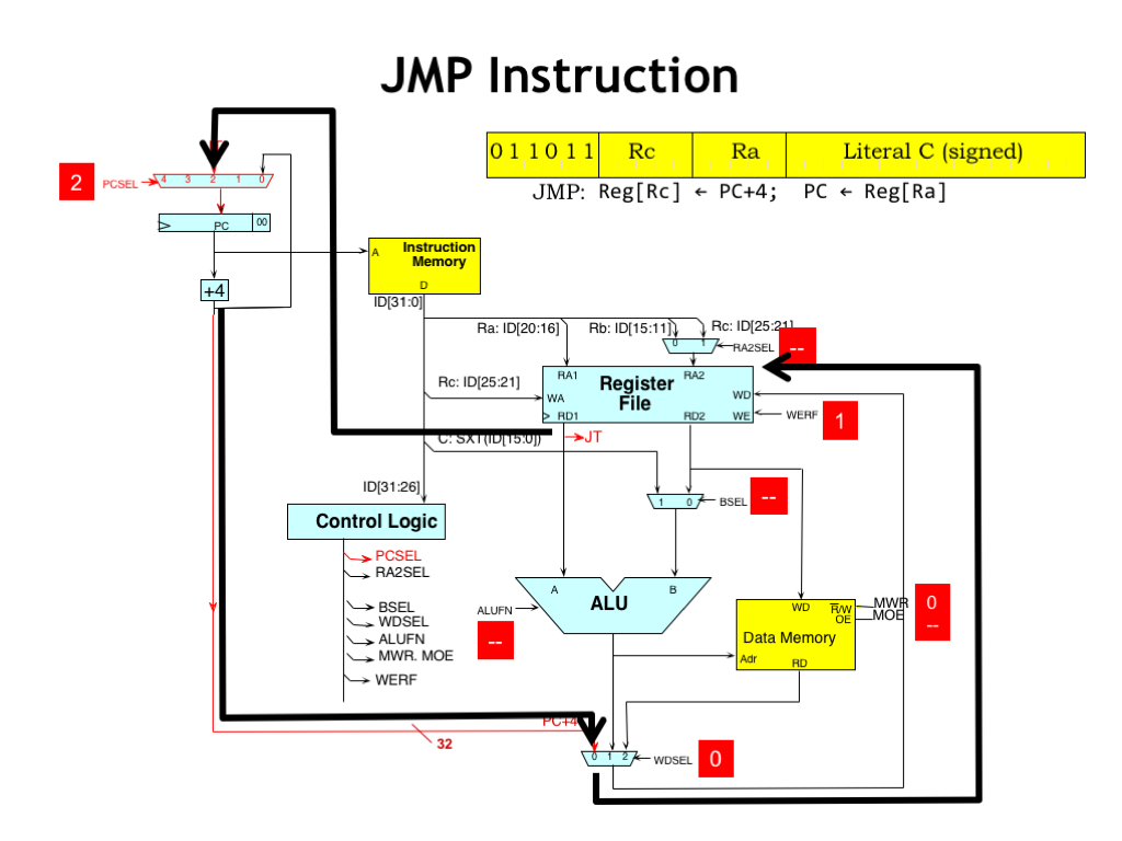
Here’s how the data flow works. The output of the PC+4 adder is is routed to the register file and WERF is set to 1 to enable that value to be written at the end of the cycle.
Meanwhile, the value of RA register coming out of the register file is connected to the “2” input of the PCSEL MUX. So setting PCSEL to 2 will select the value in the RA register as the next value for the PC.
The rest of the control signals are “don’t cares”, except, of course for the memory write enable (MWR), which can never be “don’t care” lest we cause an accidental write to some memory location.
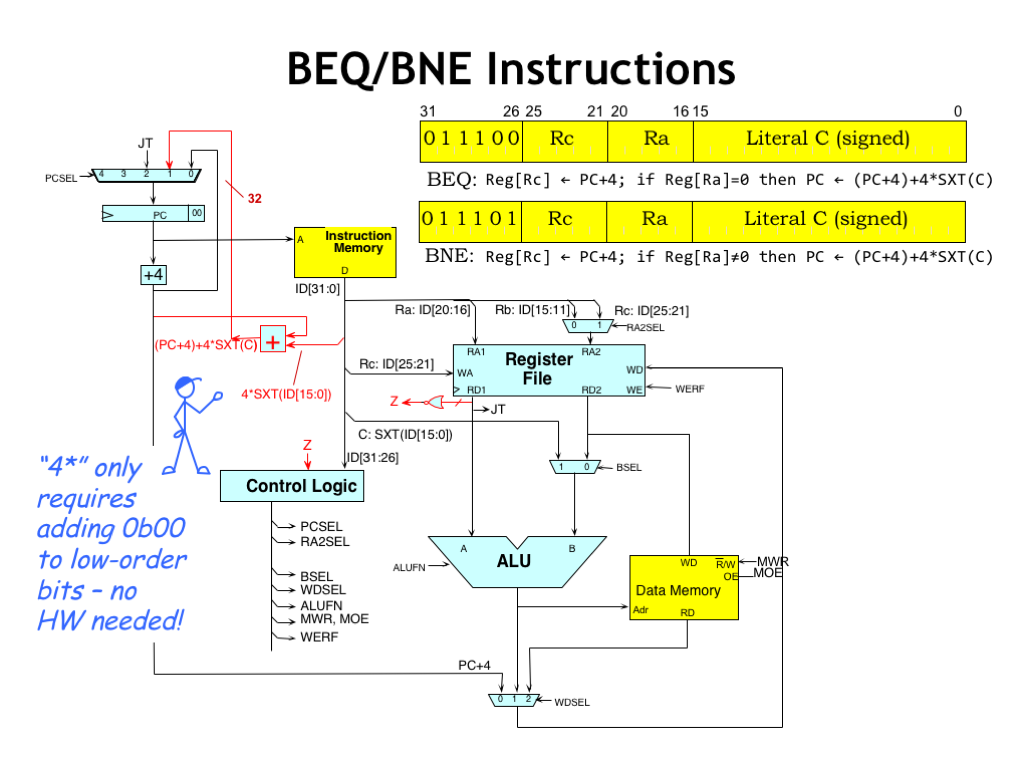
The branch instruction requires an additional adder to compute the target address by adding the scaled offset from the instruction’s literal field to the current PC+4 value. Remember that we scale the offset by a factor of 4 to convert it from the word offset stored in the literal to the byte offset required for the PC. The output of the offset adder becomes the “1” input to the PCSEL MUX, where, if the branch is taken, it will become the next value of the PC.
Note that multiplying by 4 is easily accomplished by shifting the literal two bits to the left, which inserts two 0-bits at the low-order end of the value. And, like before, the sign-extension just requires replicating bit ID[15], in this case fourteen times. So implementing this complicated-looking expression requires care in wiring up the input to the offset adder, but no additional logic!
We do need some logic to determine if we should branch or not. The 32-bit NOR gate connected to the first read port of the register file tests the value of the RA register. The NOR’s output Z will be 1 if all the bits of the RA register value are 0, and 0 otherwise.
The Z value can be used by the control logic to determine the correct value for PCSEL. If Z indicates the branch is taken, PCSEL will be 1 and the output of the offset adder becomes the next value of the PC. If the branch is not taken, PCSEL will be 0 and execution will continue with the next instruction at PC+4.
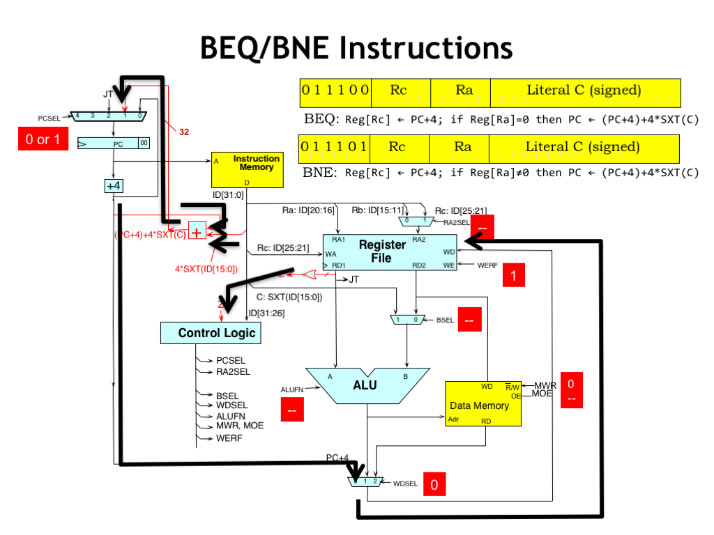
As in the JMP instruction, the PC+4 value is routed to the register file to be written into the RC register at end of the cycle.
Meanwhile, the value of Z is computed from the value of the RA register while the branch offset adder computes the address of the branch target.
The output of the offset adder is routed to the PCSEL MUX where the value of the 3-bit PCSEL control signal, computed by the control logic based on Z, determines whether the next PC value is the branch target or the PC+4 value.
The remaining control signals are unused and set to their default “don’t care” values.
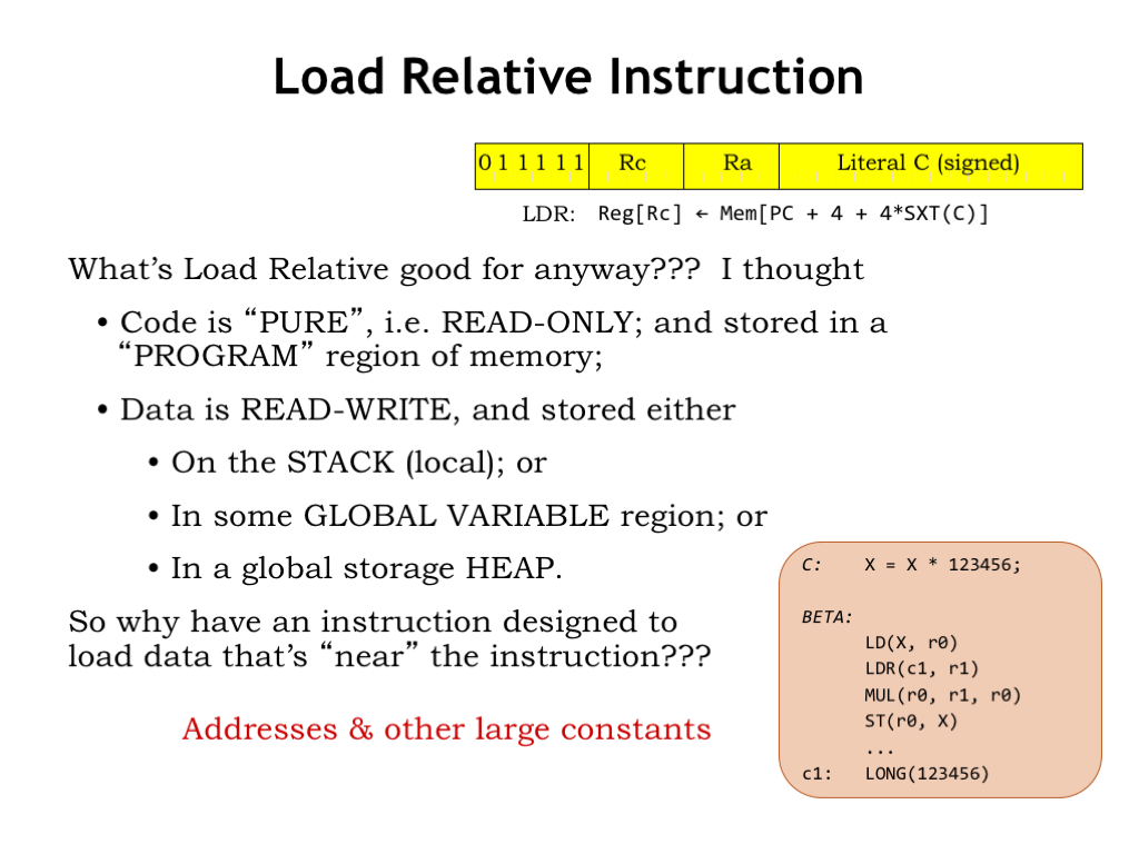
We have one last instruction to introduce: the LDR or load-relative instruction. LDR behaves like a normal LD instruction except that the memory address is taken from the branch offset adder.
Why would it be useful to load a value from a location near the LDR instruction? Normally such addresses would refer to the neighboring instructions, so why would we want to load the binary encoding of an instruction into a register to be used as data?
The use case for LDR is accessing large constants that have to be stored in main memory because they are too large to fit into the 16-bit literal field of an instruction. In the example shown here, the compiled code needs to load the constant 123456. So it uses an LDR instruction that refers to a nearby location C1: that has been initialized with the required value. Since this read-only constant is part of the program, it makes sense to store it with the instructions for the program, usually just after the code for a procedure. Note that we have to be careful to place the storage location so that it won’t be executed as an instruction!

To route the output of the offset adder to the main memory address port, we’ll add ASEL MUX so we can select either the RA register value (when ASEL=0) or the output of the offset adder (when ASEL=1) as the first ALU operand.
For LDR, ASEL will be 1, and we’ll then ask the ALU compute the Boolean operation “A”, i.e., the boolean function whose output is just the value of the first operand. This value then appears on the ALU output, which is connected to the main memory address port and the remainder of the execution proceeds just like it did for LD.
This seems a bit complicated! Mr. Blue has a good question: why not just put the ASEL MUX on the wire leading to the main memory address port and bypass the ALU altogether?
The answer has to do with the amount of time needed to compute the memory address. If we moved the ASEL MUX here, the data flow for LD and ST addresses would then pass through two MUXes: the BSEL MUX and the ASEL MUX, slowing down the arrival of the address by a small amount. This may not seem like a big deal, but the additional time would have to be added the clock period, thus slowing down every instruction by a little bit. When executing billions of instructions, a little extra time on each instruction really impacts the overall performance of the processor.
By placing the ASEL MUX where we did, its propagation delay overlaps that of the BSEL MUX, so the increased functionality it provides comes with no cost in performance.

Here’s the data flow for the LDR instruction. The output of the offset adder is routed through the ASEL MUX to the ALU. The ALU performs the Boolean computation “A” and the result becomes the address for main memory.
The returning data is routed through the WDSEL MUX so it can be written into the RC register at the end of the cycle.
The remaining control signals are given their usual default values.
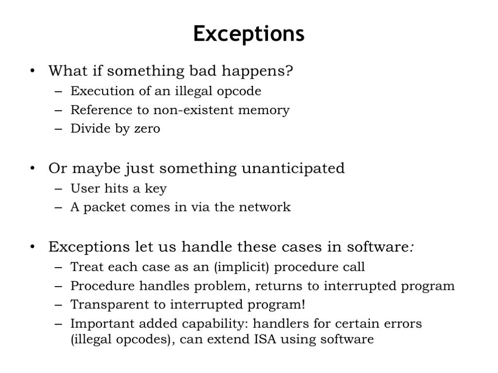
One last bit of housekeeping, then we’re done! What should our hardware do if for some reason an instruction can’t be executed? For example, if a programming error has led to trying to execute some piece of data as an instruction and the opcode field doesn’t correspond to a Beta instruction (a so-called “illop” or illegal operation). Or maybe the memory address is larger than the actual amount of main memory. Or maybe one of the operand values is not acceptable, e.g., if the B operand for a DIV instruction is 0.
In modern computers, the accepted strategy is cease execution of the running program and transfer control to some error handler code. The error handler might store the program state onto disk for later debugging. Or, for an unimplemented but legal opcode, it might emulate the missing instruction in software and resume execution as if the instruction had been implemented in hardware!
There’s also the need to deal with external events, like those associated with input and output. Here we’d like to interrupt the execution of the current program, run some code to deal with the external event, then resume execution as if the interrupt had never happened.
To deal with these cases, we’ll add hardware to treat exceptions like forced procedure calls to special code to handle the situation, arranging to save the PC+4 value of the interrupted program so that the handler can resume execution if it wishes.
This is a very powerful feature since it allows us to transfer control to software to handle most any circumstance beyond the capability of our modest hardware. As we’ll see in Part 3 of the course, the exception hardware will be our key to interfacing running programs to the operating system (OS) and to allow the OS to deal with external events without any awareness on the part of the running program.
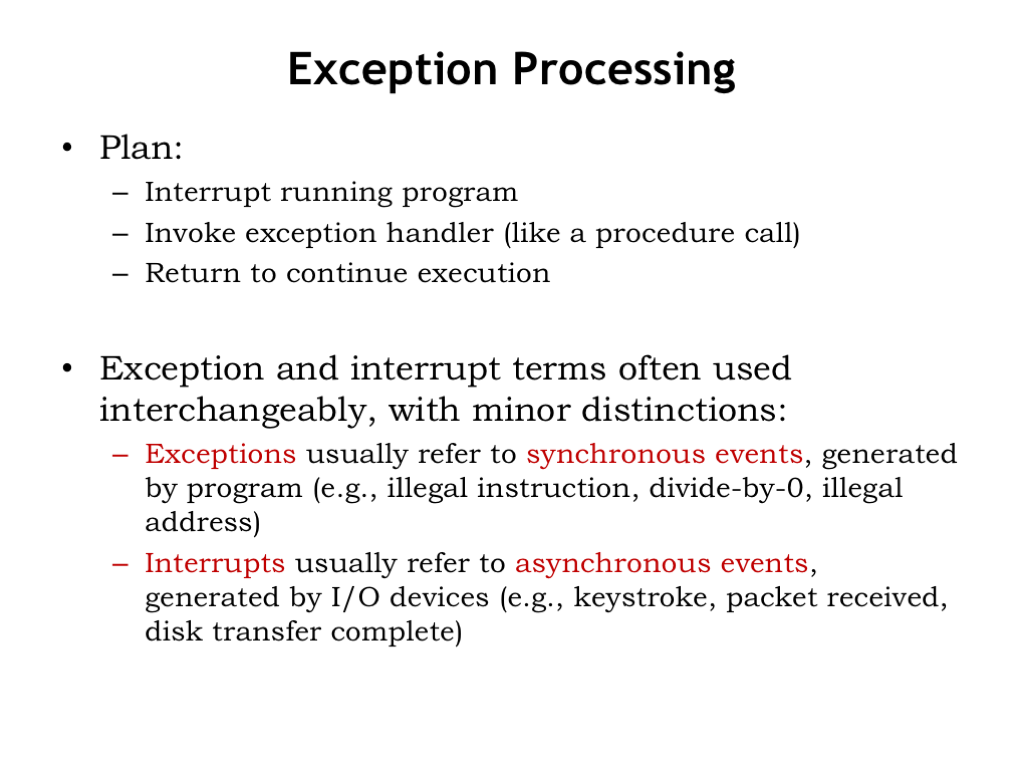
So our plan is to interrupt the running program, acting like the current instruction was actually a procedure call to the handler code. When it finishes execution, the handler can, if appropriate, use the normal procedure return sequence to resume execution of the user program.
We’ll use the term “exception” to refer to exceptions caused by executing the current program. Such exceptions are “synchronous” in the sense that they are triggered by executing a particular instruction. In other words, if the program was re-run with the same data, the same exception would occur.
We’ll use the term “interrupt” to refer to asynchronous exceptions resulting from external events whose timing is unrelated to the currently running program.

The implementation for both types of exceptions is the same. When an exception is detected, the Beta hardware will behave as if the current instruction was a taken BR to either location 0x4 (for synchronous exceptions) or location 0x8 (for asynchronous interrupts). Presumably the instructions in those locations will jump to the entry points of the appropriate handler routines.
We’ll save the PC+4 value of the interrupted program into R30, a register dedicated to that purpose. We’ll call that register XP (“exception pointer”) to remind ourselves of how we’re using it. Since interrupts in particular can happen at any point during a program’s execution, thus overwriting the contents of XP at any time, user programs can’t use the XP register to hold values since those values might disappear at any moment!
Here’s how this scheme works: suppose we don’t include hardware to implement the DIV instruction, so it’s treated as an illegal opcode. The exception hardware forces a procedure call to location 0x4, which then branches to the Illop handler shown here. The PC+4 value of the DIV instruction has been saved in the XP register, so the handler can fetch the illegal instruction and, if it can, emulate its operation in software. When handler is complete, it can resume execution of the original program at the instruction following DIV by performing a JMP(XP).
Pretty neat!
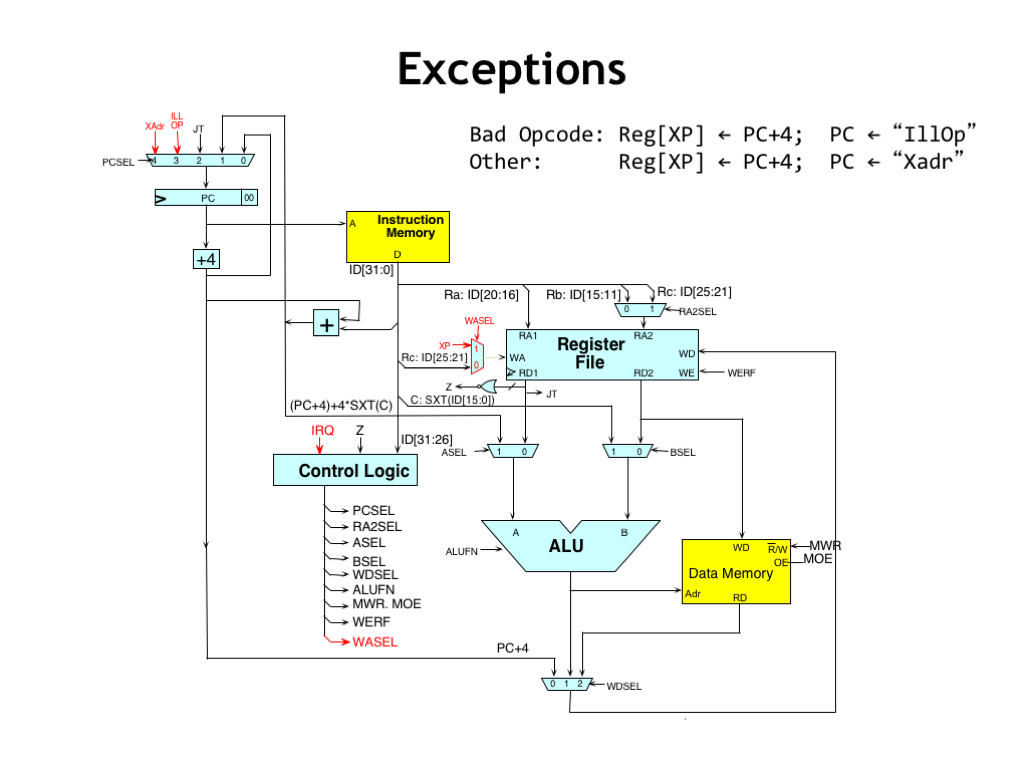
To handle exceptions, we only need a few simple changes to the datapath.
We’ve added a MUX controlled by the WASEL signal to choose the write-back address for the register file. When WASEL is 1, write-back will occur to the XP register, i.e., register 30. When WASEL is 0, write-back will occur normally, i.e., to the register specified by the RC field of the current instruction.
The remaining two inputs of the PCSEL MUX are set to the constant addresses for the exception handlers. In our case, 0x4 for illegal operations, and 0x8 for interrupts.
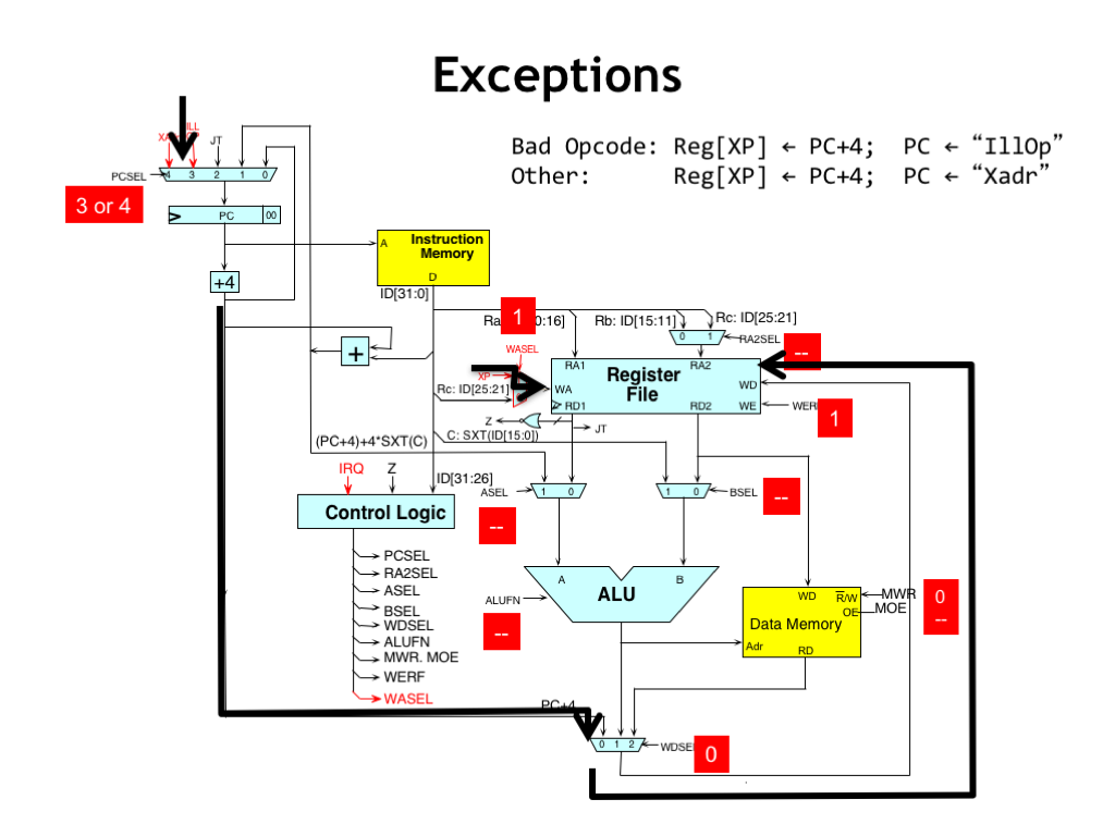
Here’s the flow of control during an exception. The PC+4 value for the interrupted instruction is routed through the WDSEL MUX to be written into the XP register. Meanwhile the control logic chooses either 3 or 4 as the value of PCSEL to select the appropriate next instruction that will initiate the handling the exception.
The remaining control signals are forced to their “don’t care” values, since we no longer care about completing execution of the instruction we had fetched from main memory at the beginning of the cycle.
Note that the interrupted instruction has not been executed. So if the exception handler wishes to execute the interrupted instruction, it will have to subtract 4 from the value in the XP register before performing a JMP(XP) to resume execution of the interrupted program.
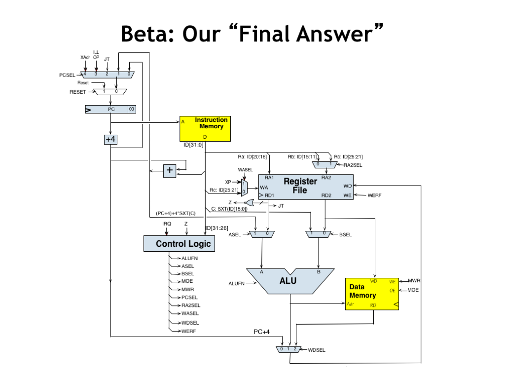
Okay, we’re done! Here’s the final datapath for executing instructions and handling exceptions. Please take a moment to remind yourself of what each datapath component does, i.e., why it was added to the datapath. Similarly, you should understand how the control signals affect the operation of the datapath.
At least to my eye, this seems like a very modest amount of hardware to achieve all this functionality! It’s so modest in fact, that I will ask you to actually complete the logic design for the Beta in an upcoming lab assignment :)
How does our design compare to the processor you’re using to view this course online? Modern processors have many additional complexities to increase performance: pipelined execution, the ability to execute more than one instruction per cycle, fancier memory systems to reduce average memory access time, etc. We’ll cover some of these enhancements in upcoming lectures. The bottom line: the Beta hardware might occupy 1 or 2 sq mm on a modern integrated circuit, while a modern Intel processor occupies 300 to 600 sq mm. Clearly all that extra circuitry is there for a reason! If you’re curious, I’d recommend taking a course on advanced processor architecture.

Here we’ve gathered up all the control signal settings for each class of instructions, including the settings needed for exceptions and during reset. Wherever possible, we’ve specified “don’t care” for control signals whose value does not affect the actions of the datapath needed for a particular instruction.
Note that the memory write enable signal always has a defined value, ensuring that we only write to the memory during ST instructions. Similarly, the write enable for the register file is well-defined, except during RESET when presumably we’re restarting the processor and don’t care about preserving any register values.
As mentioned previously, a read-only memory (ROM) indexed by the 6-bit opcode field is the easiest way to generate the appropriate control signals for the current instruction. The Z and IRQ inputs to the control logic will affect the control signals and this can be accomplished with a small amount of logic to process the ROM outputs.
One can always have fun with Karnuagh maps to generate a minimal implementation using ordinary logic gates. The result will be much smaller, both in terms of size and propagation delay, but requires a lot more design work! My recommendation: start with the ROM implementation and get everything else working. Then come back later when you feel like hacking logic gates :)

So that’s what it takes to design the hardware for a simple 32-bit computer. Of course, we made the job easy for ourselves by choosing a simple binary encoding for our instructions and limiting the hardware functionality to efficiently executing the most common operations. Less common and more complex functionality can be left to software. The exception mechanism gave us a powerful tool for transferring control to software when the hardware couldn’t handle the task.
Have fun completing the hardware design of your Beta. Thousands of MIT students have enjoyed that “Yes!” moment when their design works for the first time. For their efforts we reward them with the “Beta Inside” sticker you see here, which you can see on laptops as you walk around the Institute.
Good luck!


