L03: CMOS Technology
- Combinational Device Wish List
- N-Channel MOSFET: Physical View
- N-Channel MOSFET: Electrical View
- N-Channel MOSFET \(I_{DS}\) vs. \(V_{DS}\)
- FETs Come in Two Flavors
- CMOS Recipe
- CMOS Inverter VTC
- Beyond Inverters
- CMOS Comoplements
- A Pop Quiz!
- General CMOS Gate Recipe
- CMOS Gates Are Naturally Inverting
- CMOS Timing Specifications
- Propagation Delay
- Contamination Delay
- The Combinational Contract
- Acyclic Combinational Circuits
- One Last Timing Issue
- Lenient Gates
- Summary
Content of the following slides is described in the surrounding text.
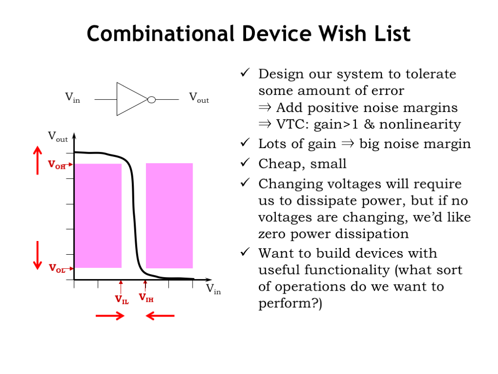
Let’s review our wish list for the characteristics of a combinational device. In the previous lecture we worked hard to develop a voltage-based representation for information that could tolerate some amount error as the information flowed through a system of processing elements.
We specified four signaling thresholds: \(V_{\textrm{OL}}\) and \(V_{\textrm{OH}}\) set the upper and lower bounds on voltages used to represent 0 and 1 respectively at the outputs of a combinational device. \(V_{\textrm{IL}}\) and \(V_{\textrm{IH}}\) served a similar role for interpreting the voltages at the inputs of a combinational device. We also specified that \(V_{\textrm{OL}}\) be strictly less than \(V_{\textrm{IL}}\), and termed the difference between these two low thresholds as the low noise margin, the amount of noise that could be added to an output signal and still have the signal interpreted correctly at any connected inputs. For the same reasons we specified that \(V_{\textrm{IH}}\) be strictly less than \(V_{\textrm{OH}}\).
We saw the implications of including noise margins when we looked at the voltage transfer characteristic — a plot of \(V_{\textrm{OUT}}\) vs. \(V_{\textrm{IN}}\) — for a combinational device. Since a combinational device must, in the steady state, produce a valid output voltage given a valid input voltage, we can identify forbidden regions in the VTC, which for valid input voltages identify regions of invalid output voltages. The VTC for a legal combinational device could not have any points that fall within these regions. The center region bounded by the four threshold voltages is narrower than it is high and so any legal VTC has to a have region where its gain is greater than 1 and the overall VTC has to be non-linear. The VTC shown here is that for a combinational device that serves as an inverter.
If we’re fortunate to be using a circuit technology that provides high gain and has output voltages close the ground and the power supply voltage, we can push \(V_{\textrm{OL}}\) and \(V_{\textrm{OH}}\) outward towards the power supply rails, and push \(V_{\textrm{IL}}\) and \(V_{\textrm{IH}}\) inward, with the happy consequence of increasing the noise margins — always a good thing!
Remembering back to the beginning of Lecture 2, we’ll be wanting billions of devices in our digital systems, so each device will have to be quite inexpensive and small.
In today’s mobile world, the ability to run our systems on battery power for long periods of time means that we’ll want to have our systems dissipate as little power as possible. Of course, manipulating information will necessitate changing voltages within the system and that will cost us some amount of power. But if our system is idle and no internal voltages are changing, we’d like for our system to have zero power dissipation.
Finally, we’ll want to be able to implement systems with useful functionality and so need to develop a catalog of the logic computations we want to perform.
Quite remarkably, there is a circuit technology that will make our wishes come true! That technology is the subject of this lecture.
The star of our show is the metal-oxide-semiconductor field-effect transistor, or MOSFET for short.
Here’s a 3D drawing showing a cross-section of a MOSFET, which is constructed from a complicated sandwich of electrical materials as part of an integrated circuit, so called because the individual devices in an integrated circuit are manufactured en-masse during a series of manufacturing steps.
In modern technologies the dimensions of the block shown here are a few 10’s of nanometers on a side — that’s 1/1000 of the thickness of a thin human hair. This dimension is so small that MOSFETs can’t be viewed using an ordinary optical microscope, whose resolution is limited by the wavelength of visible light, which is 400 to 750nm. For many years, engineers have been able to shrink the device dimensions by a factor of 2 every 24 months or so, an observation known as “Moore’s Law” after Gordon Moore, one of the founders of Intel, who first remarked on this trend in 1965. Each 50% shrink in dimensions enables integrated circuit (IC) manufacturers to build four times as many devices in the same area as before, and, as we’ll see, the devices themselves get faster too! An integrated circuit in 1975 might have had 2500 devices; today we’re able to build ICs with two to three billion devices.
Here’s a quick tour of what we see in the diagram.
The substrate upon which the IC is built is a thin wafer of silicon crystal which has had impurities added to make it conductive. In this case the impurity was an acceptor atom like Boron, and we characterize the doped silicon as a p-type semiconductor. The IC will include an electrical contact to the p-type substrate, called the bulk terminal, so we can control its voltage.
When want to provide electrical insulation between conducting materials, we’ll use a layer of silicon dioxide (SiO2). Normally the thickness of the insulator isn’t terribly important, except for when it’s used to isolate the gate of the transistor (shown here in red) from the substrate. The insulating layer in that region is very thin so that the electrical field from charges on the gate conductor can easily affect the substrate.
The gate terminal of the transistor is a conductor, in this case, polycrystalline silicon. The gate, the thin oxide insulating layer, and the p-type substrate form a capacitor, where changing the voltage on the gate will cause electrical changes in the p-type substrate directly under the gate. In early manufacturing processes the gate terminal was made of metal, and the term metal-oxide-semiconductor (MOS) is referring to this particular structure.
After the gate terminal is in place, donor atoms such as Phosphorous are implanted into the p-type substrate in two rectangular regions on either side of the gate. This changes those regions to an n-type semiconductor, which become the final two terminals of the MOSFET, called the source and the drain. Note that source and drain are usually physically identical and are distinguished by the role they play during the operation of the device, our next topic.
As we’ll see in the next slide, the MOSFET functions as a voltage-controlled switch connecting the source and drain terminals of the device. When the switch is conducting, current will flow from the drain to the source through the conducting channel formed as the second plate of the gate capacitor. The MOSFET has two critical dimensions: its length L, which measures the distance the current must cross as it flows from drain to source, and its width W, which determines how much channel is available to conduct current. The the current, termed \(I_{\textrm{DS}}\), flowing across the switch is proportional to the ratio of the channel’s width to its length.
Typically, IC designers make the length as short as possible — when a news article refers to a 14nm process, the 14nm refers to the smallest allowable value for the channel length. And designers choose the channel width to set the desired amount of current flow. If \(I_{\textrm{DS}}\) is large, voltage transitions on the source and drain nodes will be quick, at the cost of a physically larger device.
To summarize: the MOSFET has four electrical terminals: bulk, gate, source, and drain. Two of the device dimensions are under the control of the designer: the channel length, usually chosen to be as small as possible, and the channel width chosen to set the current flow to the desired value. It’s a solid-state switch — there are no moving parts and the switch operation is controlled by electrical fields determined by the relative voltages of the four terminals.
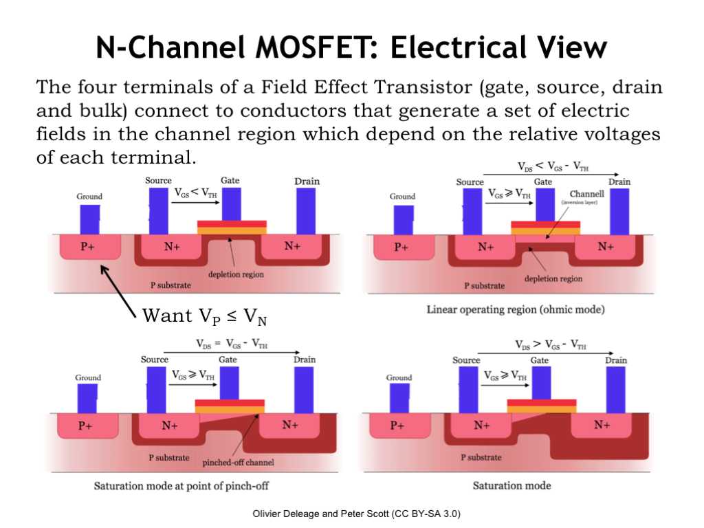
Now let’s look at the electrical view of the MOSFET. Its operation is determined by the voltages of its four terminals.
First we’ll label the two diffusion terminals on either side of the gate terminal: our convention is to call the diffusion terminal with the highest voltage potential the drain and the other lower-potential terminal the source. With this labeling if any current is flowing through the MOSFET switch, it will flow from drain to source.
When the MOSFET is manufactured, it’s designed to have a particular threshold voltage, \(V_{\textrm{TH}}\), which tells us when the switch goes from non-conducting/OFF/OPEN to conducting/ON/CLOSED. For the n-channel MOSFET shown here, we’d expect \(V_{\textrm{TH}}\) to be around 0.5V in a modern process.
The P+ terminal on the left of the diagram is the connection to the p-type substrate. For the MOSFET to operate correctly, the substrate must always have a voltage less than or equal to the voltage of the source and drain. We’ll have specific rules about how to connect up this terminal.
The MOSFET is controlled by the difference between the voltage of the gate, \(V_G\), and the voltage of the source, \(V_S\), which, following the usual terminology for voltages we call \(V_{\textrm{GS}}\), a shortcut for saying \(V_G - V_S\).
The first picture shows the configuration of the MOSFET when \(V_{\textrm{GS}}\) is less than the MOSFET’s threshold voltage. In this configuration, the switch is open or non-conducting, i.e., there is no electrical connection between the source and drain.
When n-type and p-type materials come in physical contact, a depletion region (shown in dark red in the diagram) forms at their junction. This is a region of substrate where the current-carrying electrical particles have migrated away from the junction. The depletion zone serves as an insulating layer between the substrate and source/drain. The width of this insulating layer grows as the voltage of source/drain gets larger relative to the voltage of the substrate. And, as you can see in the diagram, that insulating layer fills the region of the substrate between the source and drain terminals, keeping them electrically isolated.
Now, as \(V_{\textrm{GS}}\) gets larger, positive charges accumulate on the gate conductor and generate an electrical field which attracts the electrons in the atoms in the substrate. For a while that attractive force gets larger without much happening, but when it reaches the MOSFET’s threshold voltage, the field is strong enough to pull the substrate electrons from the valence band into the conduction band, and the newly mobile electrons will move towards the gate conductor, collecting just under the thin oxide that serves the gate capacitor’s insulator.
When enough electrons accumulate, the type of the semiconductor changes from p-type to n-type and there’s now a channel of n-type material forming a conducting path between the source and drain terminals. This layer of n-type material is called an inversion layer, since its type has been inverted from the original p-type material. The MOSFET switch is now closed or conducting. Current will flow from drain to source in proportion to \(V_{\textrm{DS}}\), the difference in voltage between the drain and source terminals.
At this point the conducting inversion layer is acting like a resistor governed by Ohm’s Law so \(I_{DS} = V_{DS}/R\) where R is the effective resistance of the channel. This process is reversible: if \(V_{\textrm{GS}}\) falls below the threshold voltage, the substrate electrons drop back into the valence band, the inversion layer disappears, and the switch no longer conducts.
The story gets a bit more complicated when \(V_{\textrm{DS}}\) is larger than \(V_{\textrm{GS}}\), as shown in the bottom figures. A large \(V_{\textrm{DS}}\) changes the geometry of the electrical fields in the channel and the inversion layer pinches off at the end of the channel near the drain. But with a large \(V_{\textrm{DS}}\), the electrons will tunnel across the pinch-off point to reach the conducting inversion layer still present next to the source terminal.
How does pinch-off affect \(I_{\textrm{DS}}\), the current flowing from drain to source? To see, let’s look at some plots of \(I_{\textrm{DS}}\) on the next slide.
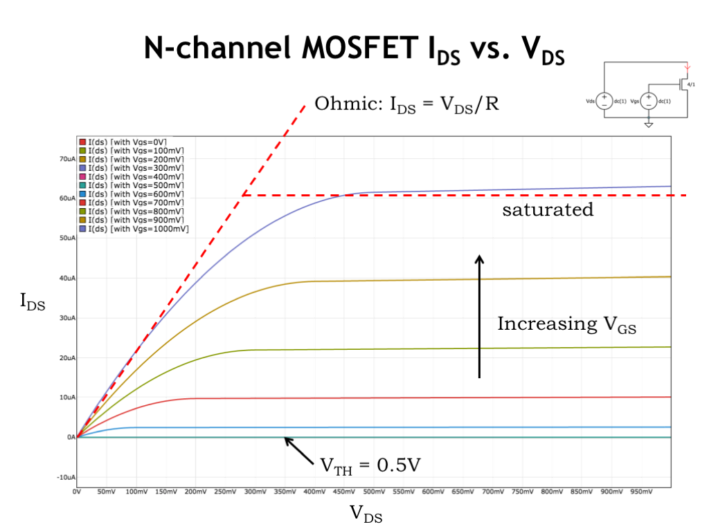
Okay, this plot has a lot of information, so let’s see what we can learn. Each curve is a plot of \(I_{\textrm{DS}}\) as a function of \(V_{\textrm{DS}}\), for a particular value of \(V_{\textrm{GS}}\). First, notice that \(I_{\textrm{DS}}\) is 0 when \(V_{\textrm{GS}}\) is less than or equal to the threshold voltage. The first six curves are all plotted on top of each other along the x-axis.
Once \(V_{\textrm{GS}}\) exceeds the threshold voltage \(I_{\textrm{DS}}\) becomes non-zero, and increases as \(V_{\textrm{GS}}\) increases. This makes sense: the larger \(V_{\textrm{GS}}\) becomes, the more substrate electrons are attracted to the bottom plate of the gate capacitor and the thicker the inversion layer becomes, allowing it to conduct more current. When \(V_{\textrm{DS}}\) is smaller than \(V_{\textrm{GS}}\), we said the MOSFET behaves like a resistor obeying Ohm’s Law. This is shown in the linear portions of the \(I_{\textrm{DS}}\) curves at the left side of the plots. The slope of the linear part of the curve is essentially inversely proportional to the resistance of the conducting MOSFET channel. As the channel gets thicker with increasing \(V_{\textrm{GS}}\), more current flows and the slope of the line gets steeper, indicating a smaller channel resistance.
But when \(V_{\textrm{DS}}\) gets larger than \(V_{\textrm{GS}}\), the channel pinches off at the drain end and, as we see in on the right side of the \(I_{\textrm{DS}}\) plots, the current flow no longer increases with increasing \(V_{\textrm{DS}}\). Instead \(I_{\textrm{DS}}\) is approximately constant and the curve becomes a horizontal line. We say that the MOSFET has reached saturation where \(I_{\textrm{DS}}\) has reached some maximum value.
Notice that the saturated part of the \(I_{\textrm{DS}}\) curve isn’t quite flat and \(I_{\textrm{DS}}\) continues to increase slightly as \(V_{\textrm{DS}}\) gets larger. This effect is called channel-length modulation and reflects the fact that the increase in channel pinch-off isn’t exactly matched by the increase current induced by the larger \(V_{\textrm{DS}}\).
Whew! MOSFET operation is complicated! Fortunately, as designers, we’ll be able to use the much simpler mental model of a switch if we obey some simple rules when designing our MOSFET circuits.
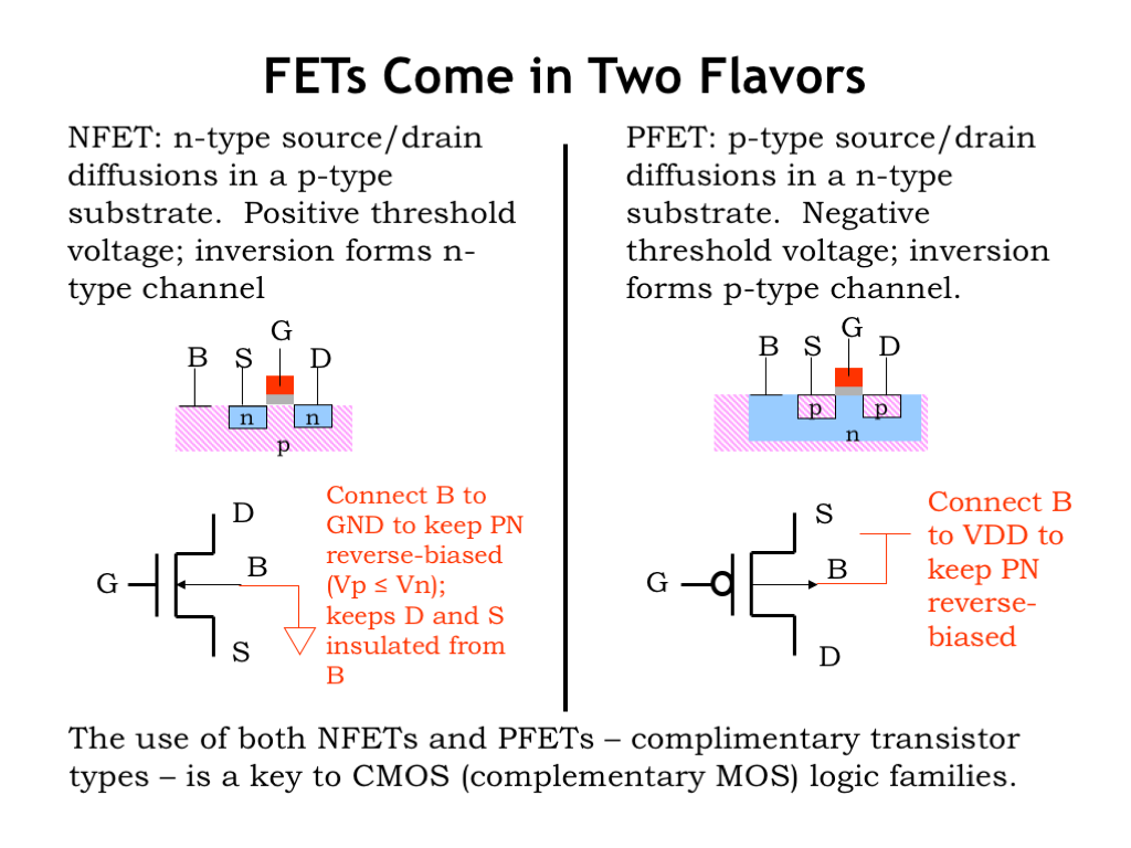
Up to now, we’ve been talking about MOSFETs built as shown in the diagram on the left: with n-type source/drain diffusions in a p-type substrate. These are called n-channel MOSFETs since the inversion layer, when formed, is an n-type semiconductor. The schematic symbol for an n-channel MOSFET is shown here, with the four terminals arranged as shown. In our MOSFET circuits, we’ll connect the bulk terminal of the MOSFET to ground, which will ensure that the voltage of the p-type substrate is always less than or equal to the voltage of the source and drain diffusions.
We can also build a MOSFET by flipping all the material types, creating p-type source/drain diffusions in a n-type substrate. This is called a p-channel MOSFET, which also behaves as voltage-controlled switch, except that all the voltage potentials are reversed! As we’ll see, control voltages that cause an n-channel switch to be ON will cause a p-channel switch to be OFF and vice-versa.
Using both types of MOSFETs will give us switches that behave in a complementary fashion. Hence the name complementary MOS, CMOS for short, for circuits that use both types of MOSFETs. Now that we have our two types of voltage-controlled switches, our next task is to figure out how to use them to build circuits useful for manipulating information encoded as voltages.
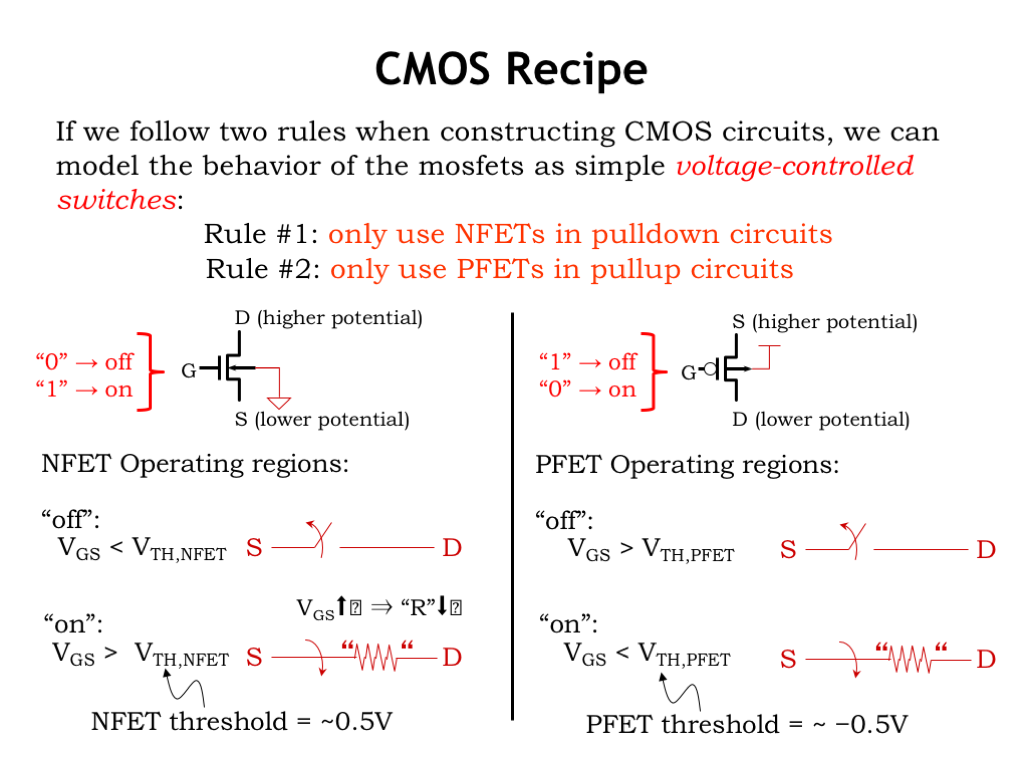
Now that we have some sense about how MOSFETs function, let’s use them to build circuits to process our digitally encoded information. We have two simple rules we’ll use when building the circuits, which, if they’re followed, will allow us to abstract the behavior of the MOSFET as a simple voltage-controlled switch.
The first rule is that we’ll only use n-channel MOSFETs, which we’ll call NFETs for short, when building pulldown circuits that connect a signaling node to the GND rail of the power supply. When the pulldown circuit is conducting, the signaling node will be at 0V and qualify as a digital 0.
If we obey this rule, NFETs will act switches controlled by \(V_{\textrm{GS}}\), the difference between the voltage of the gate terminal and the voltage of the source terminal. When \(V_{\textrm{GS}}\) is lower than the MOSFET’s threshold voltage, the switch is OPEN or not conducting and there is no connection between the MOSFET’s source and drain terminals. If \(V_{\textrm{GS}}\) is greater than the threshold voltage, the switch is ON or conducting and there is a connection between the source and drain terminals. That path has a resistance determined by the magnitude of \(V_{\textrm{GS}}\). The larger \(V_{\textrm{GS}}\), the lower the effective resistance of the switch and the more current that will flow from drain to source. When designing pulldown circuits of NFET switches, we can use the following simple mental model for each NFET switch: if the gate voltage is a digital 0, the switch will be off; if the gate voltage is a digital 1, the switch will be on.
The situation with PFET switches is analogous, except that the potentials are reversed. Our rule is that PFETs can only be used in pullup circuits, used to connect a signaling node to the power supply voltage, which we’ll call \(V_{\textrm{DD}}\). When the pullup circuit is conducting, the signaling node will be at \(V_{\textrm{DD}}\) volts and qualify as a digital 1. PFETs have a negative threshold voltage and \(V_{\textrm{GS}}\) has to be less than the threshold voltage in order for the PFET switch to be conducting. All these negatives can be a bit confusing, but, happily there’s a simple mental model we can use for each PFET switch in the pullup circuit: if the gate voltage is a digital 0, the switch will be on; if the gate voltage is a digital 1, the switch will be off — basically the opposite behavior of the NFET switch.
You may be wondering why we can’t use NFETs in pullup circuits or PFETs in pulldown circuits. You’ll get to explore the answer to this question in one of the lab assignments. Meanwhile, the short answer is that the signaling node will experience degraded signaling levels and we’ll loose the noise margins we’ve worked so hard to create!
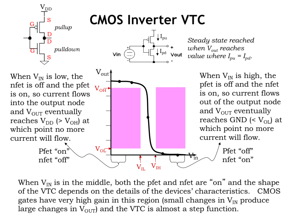
Now consider the CMOS implementation of a combinational inverter. If the inverter’s input is a digital 0, its output is a digital 1, and vice versa. The inverter circuit consists of a single NFET switch for the pulldown circuit, connecting the output node to GND and a single PFET switch for the pullup circuit, connecting the output to \(V_{\textrm{DD}}\). The gate terminals of both switches are connected to the inverter’s input node. The inverter’s voltage transfer characteristic is shown in the figure.
When \(V_{\textrm{IN}}\) is a digital 0 input, we see that \(V_{\textrm{OUT}}\) is greater than or equal to \(V_{\textrm{OH}}\), representing a digital 1 output. Let’s look at the state of the pullup and pulldown switches when the input is a digital 0. Recalling the simple mental model for the NFET and PFET switches, a 0-input means the NFET switch is off, so there’s no connection between the output node and ground, and the PFET switch is on, making a connection between the output node and \(V_{\textrm{DD}}\). Current will flow through the pullup switch, charging the output node until its voltage reaches \(V_{\textrm{DD}}\). Once both the source and drain terminals are at \(V_{\textrm{DD}}\), there’s no voltage difference across the switch and hence no more current will flow through the switch.
Similarly, when \(V_{\textrm{IN}}\) is a digital 1, the NFET switch is on and PFET switch is off, so the output is connected to ground and eventually reaches a voltage of 0V. Again, current flow through pulldown switch will cease once the output node reaches 0V.
When the input voltage is in the middle of its range, it’s possible, depending on the particular power supply voltage used and the threshold voltage of the MOSFETs, that both the pullup and pulldown circuits will be conducting for a short period of time. That’s okay. In fact, with both MOSFET switches on, small changes in the input voltage will produce large changes in the output voltage, leading to the very high gain exhibited by CMOS devices. This in turn will mean we can pick signaling thresholds that incorporate generous noise margins, allowing CMOS devices to work reliably in many different operating environments.
This is our first CMOS combinational logic gate. In the next slide, we’ll explore how to build other, more interesting logic functions.
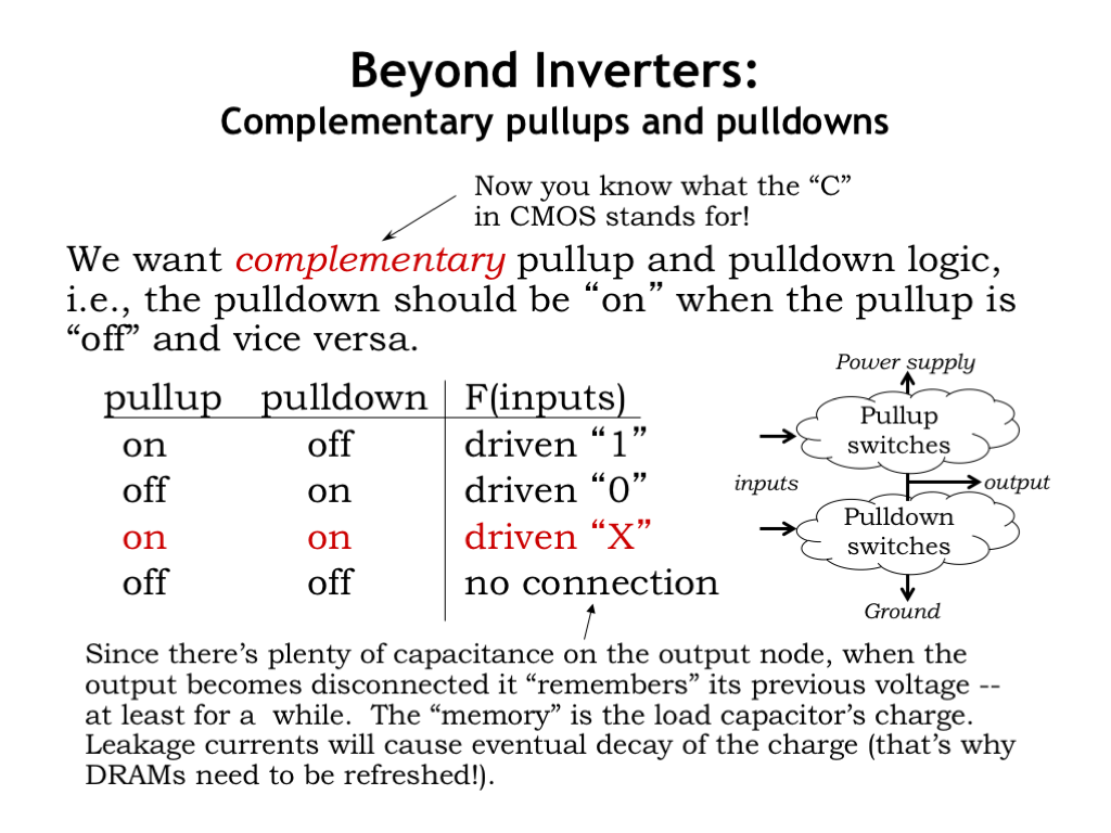
Now we get to the fun part! To build other logic gates, we’ll design complementary pullup and pulldown circuits, hooked up as shown in the diagram on the right, to control the voltage of the output node. Complementary refers to property that when one of the circuits is conducting, the other is not. When the pullup circuit is conducting and the pulldown circuit is not, the output node has a connection to \(V_{\textrm{DD}}\) and its output voltage will quickly rise to become a valid digital 1 output. Similarly, when the pulldown circuit is conducting and the pullup is not, the output node has a connection to GND and its output voltage will quickly fall to become a valid digital 0 output.
If the circuits are incorrectly designed so that they are not complementary and could both be conducting for an extended period of time, there’s a path between \(V_{\textrm{DD}}\) and GND and large amounts of short circuit current will flow, a very bad idea. Since our simple switch model won’t let us determine the output voltage in this case, we’ll call this output value X or unknown.
Another possibility with a non-complementary pullup and pulldown is that neither is conducting and the output node has no connection to either power supply voltage. At this point, the output node is electrically floating and whatever charge is stored by the nodal capacitance will stay there, at least for a while. This is a form of memory and we’ll come back to this in a couple of lectures.
For now, we’ll concentrate on the behavior of devices with complementary pullups and pulldowns.
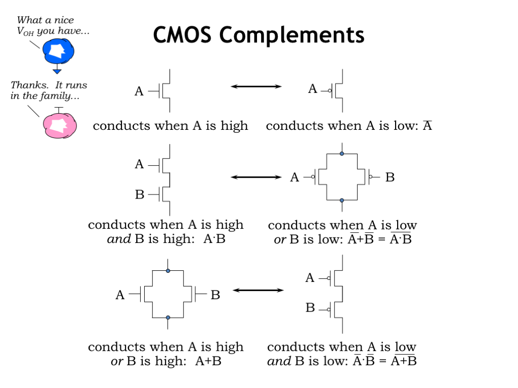
Since the pullup and pulldown circuits are complementary, we’ll see there’s a nice symmetry in their design. We’ve already seen the simplest complementary circuit: a single NFET pulldown and a single PFET pullup. If the same signal controls both switches, it’s easy to see that when one switch is on, the other switch is off.
Now consider a pulldown circuit consisting of two NFET switches in series. There’s a connection through both switches when A is 1 and B is 1. For any other combination of A and B values, one or the other of the switches (or both!) will be off. The complementary circuit to NFET switches in series is PFET switches in parallel. There’s a connection between the top and bottom circuit nodes when either of the PFET switches is on, i.e., when A is 0 or B is 0. As a thought experiment consider all possible pairs of values for A and B: 00, 01, 10, and 11. When one or both of the inputs is 0, the series NFET circuit is not conducting and parallel PFET circuit is. And when both inputs are 1, the series NFET circuit is conducting but the parallel PFET circuit is not.
Finally consider the case where we have parallel NFETs and series PFETs. Conduct the same thought experiment as above to convince yourself that when one of the circuits is conducting the other isn’t.
Let’s put these observations to work when building our next CMOS combinational device.
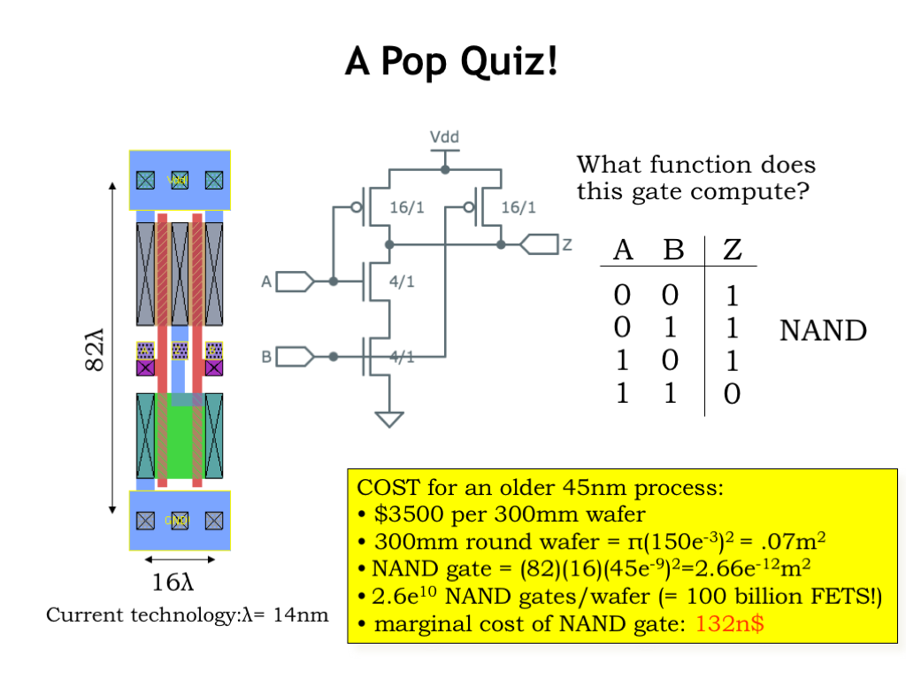
In this device, we’re using series NFETs in the pulldown and parallel PFETs in the pullup, circuits that we convinced ourselves were complementary in the previous slide. We can build a tabular representation, called a truth table, that describes the value of Z for all possible combinations of the input values for A and B.
When A and B are 0, the PFETs are on and the NFETs are off, so Z is connected to \(V_{\textrm{DD}}\) and the output of the device is a digital 1. In fact, if either A or B is 0 that continues to be the case, and the value of Z is still 1. Only when both A and B are 1 will both NFETs be on and the value of Z become 0. This particular device is called a NAND gate, short for NOT-AND, a function that is the inverse of the AND function.
Returning to a physical view for a moment, the figure on the left is a bird’s eye view, looking down on the surface of the integrated circuit, showing how the MOSFETs are laid out in two dimensions. The blue material represents metal wires with large top and bottom metal runs connecting to \(V_{\textrm{DD}}\) and GND. The red material forms the polysilicon gate nodes, the green material the n-type source/drain diffusions for the NFETs and the tan material the p-type source/drain diffusions for the PFETs.
Can you see that the NFETs are connected in series and the PFETs in parallel?
Just to give you a sense of the costs of making a single NAND gate, the yellow box is a back-of-the-envelope calculation showing that we can manufacture approximately 26 billion NAND gates on a single 300mm (that’s 12 inches for us non-metric folks) silicon wafer. For the older IC manufacturing process shown here, it costs about \(\\)\(3500 to buy the materials and perform the manufacturing steps needed to form the circuitry for all those NAND gates. So the final cost is a bit more than 100 nano-dollars per NAND gate. I think this qualifies as both cheap and small!
Using more complicated series/parallel networks of switches, we can build devices that implement more complex logic functions.
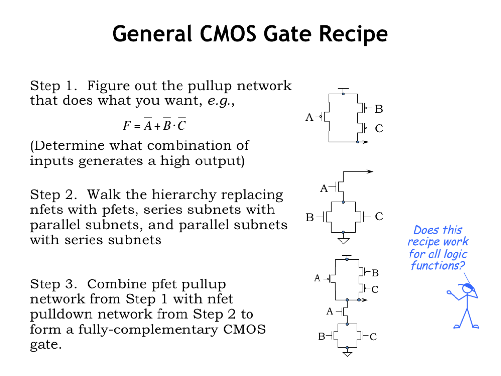
To design a more complex logic gate, first figure the series and parallel connections of PFET switches that will connect the gate’s output to \(V_{\textrm{DD}}\) for the right combination of inputs. In this example, the output F will be 1 when A is 0 OR when both B is 0 AND C is 0. The OR translates into a parallel connection, and the AND translates into a series connection, giving the pullup circuit you see to the right.
To build the complementary pulldown circuit, systematically walk the hierarchy of pullup connections, replacing PFETs with NFETs, series subcircuits with parallel subcircuits, and parallel subcircuits with series subcircuits. In the example shown, the pullup circuit had a switch controlled by A in parallel with a series subcircuit consisting of switches controlled by B and C. The complementary pulldown circuit uses NFETs, with the switch controlled by A in series with a parallel subcircuit consisting of switches controlled by B and C.
Finally combine the pullup and pulldown circuits to form a fully-complementary CMOS implementation. This probably went by a bit quickly, but with practice you’ll get comfortable with the CMOS design process.
Mr. Blue is asking a good question: will this recipe work for any and all logic functions? The answer is “no,” let’s see why.
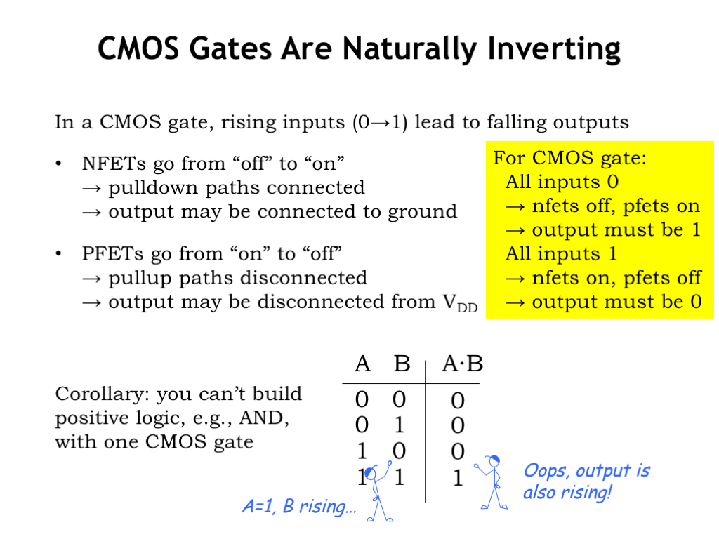
Using CMOS, a single gate (a circuit with one pullup network and one pulldown network) can only implement the so-called inverting functions where rising inputs lead to falling outputs and vice versa. To see why, consider what happens with one of the gate’s inputs goes from 0 to 1.
Any NFET switches controlled by the rising input will go from OFF to ON. This may enable one or more paths between the gate’s output and GND. And PFET switches controlled by the rising input will go from ON to OFF. This may disable one or more paths between the gate’s output and \(V_{\textrm{DD}}\). So if the gate’s output changes as the result of the rising input, it must be because some pulldown path was enabled and some pullup path was disabled. In other words, any change in the output voltage due to a rising input must be a falling transition from 1 to 0.
Similar reasoning tells us that falling inputs must lead to rising outputs. In fact, for any non-constant CMOS gate, we know that its output must be 1 when all inputs are 0 (since all the NFETs are off and all the PFETs are on). And vice-versa: if all the inputs are 1, the gate’s output must be 0. This means that so-called positive logic can’t be implemented with a single CMOS gate.
Look at this truth table for the AND function. It’s value when both inputs are 0 or both inputs are 1 is inconsistent with our deductions about the output of a CMOS gate for these combinations of inputs. Furthermore, we can see that when A is 1 and B rises from 0 to 1, the output rises instead of falls. Moral of the story: when you’re a CMOS designer, you’ll get very good at implementing functionality with inverting logic!
Okay, now that we understand how to build combinational logic gates using CMOS, let’s turn our attention to the timing specifications for the gates.
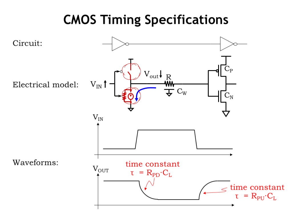
Here’s a simple circuit consisting of two CMOS inverters connected in series, which we’ll use to understand how to characterize the timing of the inverter on the left. It will be helpful to build an electrical model of what happens when we change \(V_{\textrm{IN}}\), the voltage on the input to the left inverter. If \(V_{\textrm{IN}}\) makes a transition from a digital 0 to a digital 1, the PFET switch in the pullup turns off and the NFET switch in pulldown turns on, connecting the output node of the left inverter to GND.
The electrical model for this node includes the distributed resistance and capacitance of the physical wire connecting the output of the left inverter to the input of the right inverter. And there is also capacitance associated with the gate terminals of the MOSFETs in the right inverter. When the output node is connected to GND, the charge on this capacitance will flow towards the GND connection through the resistance of the wire and the resistance of the conducting channel of the NFET pulldown switch. Eventually the voltage on the wire will reach the potential of the GND connection, 0V. The process is much the same for falling transitions on \(V_{\textrm{IN}}\), which cause the output node to charge up to \(V_{\textrm{DD}}\).
Now let’s look at the voltage waveforms as a function of time.
The top plot shows both a rising and, later, a falling transition for \(V_{\textrm{IN}}\). We see that the output waveform has the characteristic exponential shape for the voltage of a capacitor being discharged or charged though a resistor. The exponential is characterized by its associated R-C time constant, where, in this case, the R is the net resistance of the wire and MOSFET channel, and the C is the net capacitance of the wire and MOSFET gate terminals. Since neither the input nor output transition is instantaneous, we have some choices to make about how to measure the inverter’s propagation delay. Happily, we have just the guidance we need from our signaling thresholds!
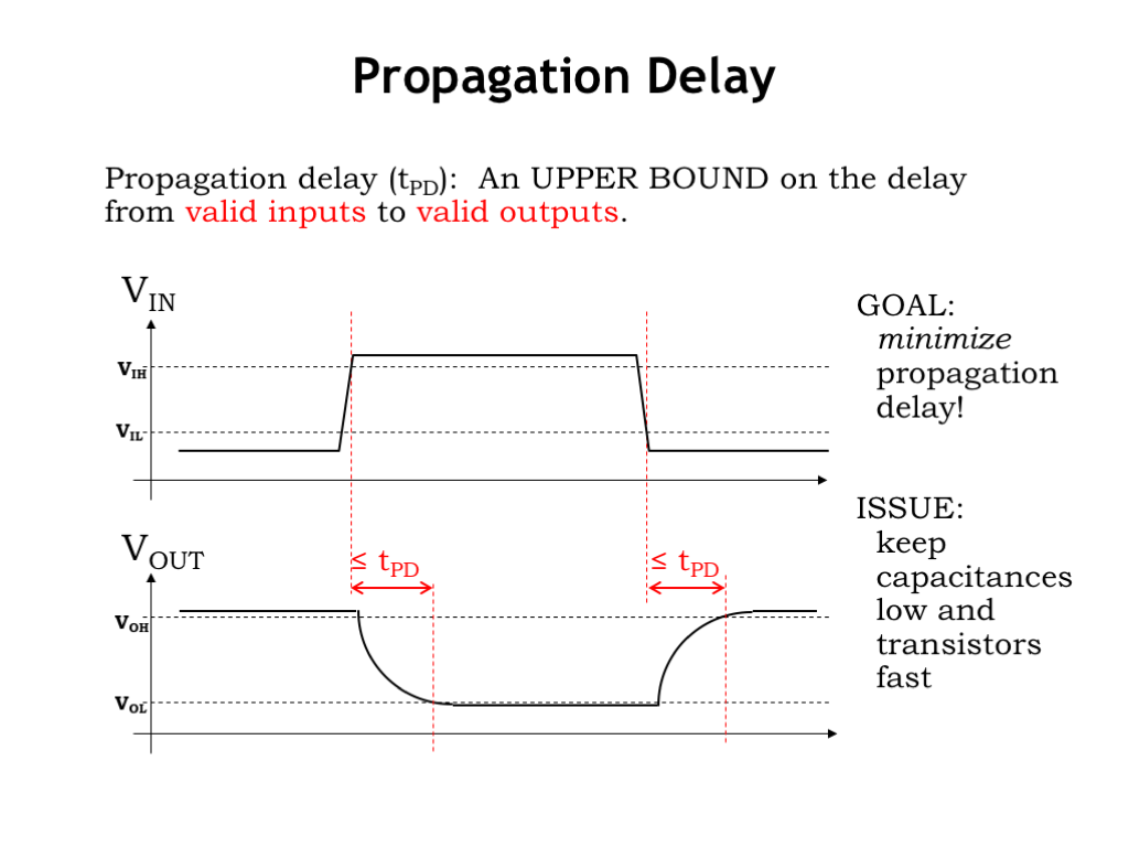
The propagation delay of a combinational logic gate is defined to be an upper bound on the delay from valid inputs to valid outputs. Valid input voltages are defined by the \(V_{\textrm{IL}}\) and \(V_{\textrm{IH}}\) signaling thresholds, and valid output voltages are defined by the \(V_{\textrm{OL}}\) and \(V_{\textrm{OH}}\) signaling thresholds. We’ve shown these thresholds on the waveform plots.
To measure the delay associated with the rising transition on \(V_{\textrm{IN}}\), first identify the time when the input becomes a valid digital 1, i.e., the time at which \(V_{\textrm{IN}}\) crosses the \(V_{\textrm{IH}}\) threshold. Next identify the time when the output becomes a valid digital 0, i.e., the time at which \(V_{\textrm{OUT}}\) crosses the \(V_{\textrm{OL}}\) threshold. The interval between these two time points is the delay for this particular set of input and output transitions.
We can go through the same process to measure the delay associated with a falling input transition. First, identify the time at which \(V_{\textrm{IN}}\) cross the \(V_{\textrm{IL}}\) threshold. Then find the time at which \(V_{\textrm{OUT}}\) crosses the \(V_{\textrm{OH}}\) threshold. The resulting interval is the delay we wanted to measure.
Since the propagation delay, \(t_{\textrm{PD}}\), is an upper bound on the delay associated with any input transition, we’ll choose a value for \(t_{\textrm{PD}}\) that’s greater than or equal to the measurements we just made. When a manufacturer selects the \(t_{\textrm{PD}}\) specification for a gate, it must take into account manufacturing variations, the effects of different environmental conditions such as temperature and power-supply voltage, and so on. It should choose a \(t_{\textrm{PD}}\) that will be an upper bound on any delay measurements their customers might make on actual devices.
From the designer’s point of view, we can rely on this upper bound for each component of a larger digital system and use it to calculate the system’s \(t_{\textrm{PD}}\) without having to repeat all the manufacturer’s measurements. If our goal is to minimize the propagation delay of our system, then we’ll want to keep the capacitances and resistances as small as possible. There’s an interesting tension here: to make the effective resistance of a MOSFET switch smaller, we would increase its width. But that would add additional capacitance to the switch’s gate terminal, slowing down transitions on the input node that connects to the gate! It’s a fun optimization problem to figure out transistor sizing that minimizes the overall propagation delay.
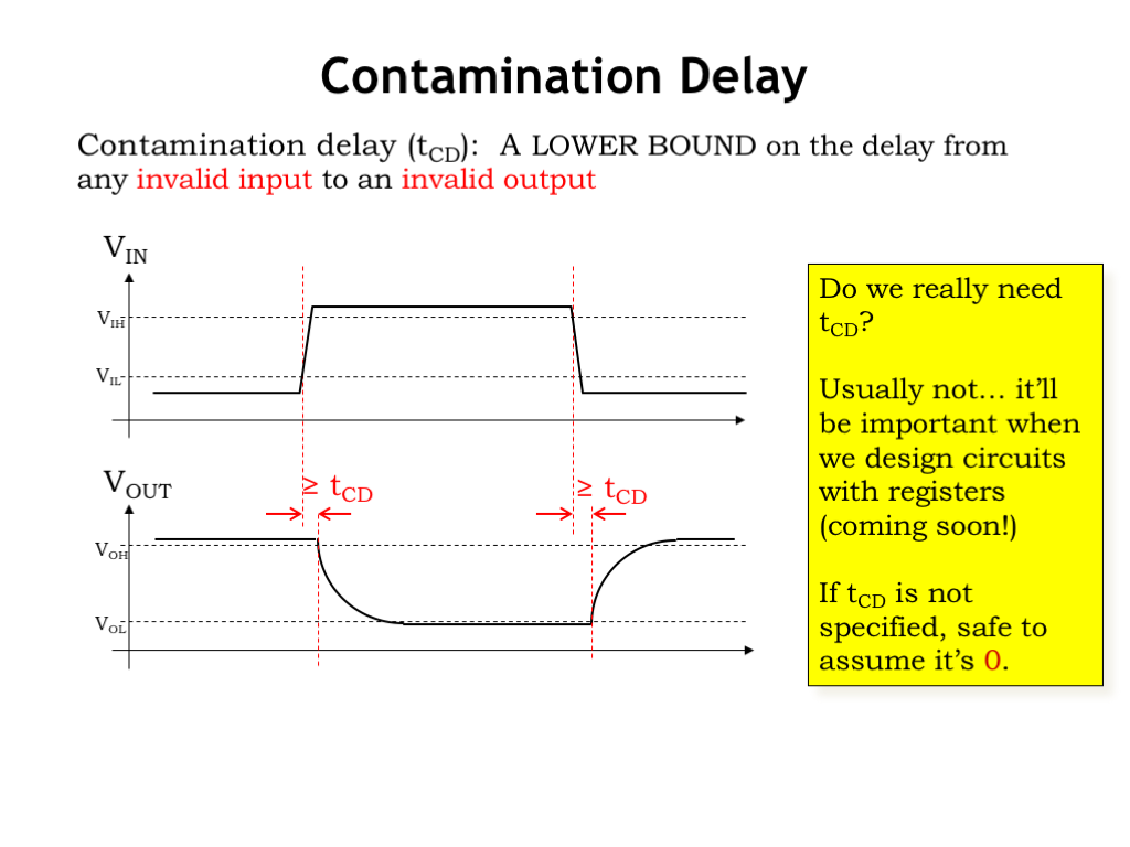
Although not strictly required by the static discipline, it will be useful to define another timing specification, called the contamination delay. It measures how long a gate’s previous output value remains valid after the gate’s inputs start to change and become invalid. Technically, the contamination delay will be a lower bound on the delay from an invalid input to an invalid output. We’ll make the delay measurements much as we did for the propagation delay.
On a rising input transition, the delay starts when the input is no longer a valid digital 0, i.e., when \(V_{\textrm{IN}}\) crosses the \(V_{\textrm{IL}}\) threshold. And the delay ends when the output becomes invalid, i.e., when \(V_{\textrm{OUT}}\) crosses the \(V_{\textrm{OH}}\) threshold. We can make a similar delay measurement for the falling input transition. Since the contamination delay, \(t_{\textrm{CD}}\), is a lower bound on the delay associated with any input transition, we’ll choose a value for \(t_{\textrm{CD}}\) that’s less than or equal to the measurements we just made.
Do we really need the contamination delay specification? Usually not. And if not’s specified, designers should assume that the \(t_{\textrm{CD}}\) for a combinational device is 0. In other words a conservative assumption is that the outputs go invalid as soon as the inputs go invalid.
By the way, manufacturers often use the term “minimum propagation delay” to refer to a device’s contamination delay. That terminology is a bit confusing, but now you know what it is they’re trying to tell you.
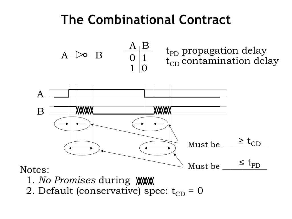
So here’s a quick summary of the timing specifications for combinational logic. These specifications tell us how the timing of changes in the output waveform (labeled B in this example) are related to the timing of changes in the input waveform (labeled A).
A combinational device may retain its previous output value for some interval of time after an input transition. The contamination delay of the device is a guarantee on the minimum size of that interval, i.e., \(t_{\textrm{CD}}\) is a lower bound on how long the old output value stays valid. As stated in Note 2, a conservative assumption is that the contamination delay of a device is 0, meaning the device’s output may change immediately after an input transition. So \(t_{\textrm{CD}}\) gives us information on when B will start to change.
Similarly, it would be good to know when B is guaranteed to be done changing after an input transition. In other words, how long do we have to wait for a change in the inputs to reflected in an updated value on the outputs? This is what \(t_{\textrm{PD}}\) tells us since it is a upper bound on the time it takes for B to become valid and stable after an input transition.
As Note 1 points out, in general there are no guarantees on the behavior of the output in the interval after \(t_{\textrm{CD}}\) and before \(t_{\textrm{PD}}\), as measured from the input transition. It would legal for the B output to change several times in that interval, or even have a non-digital voltage for any part of the interval. As we’ll see in the last part of this lecture, we’ll be able to offer more insights into B’s behavior in this interval for a subclass of combinational devices. But in general, a designer should make no assumptions about B’s value in the interval between \(t_{\textrm{CD}}\) and \(t_{\textrm{PD}}\).
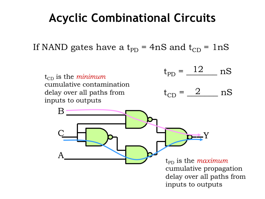
How do we calculate the propagation and contamination delays of a larger combinational circuit from the timing specifications of its components?
Our example is a circuit of four NAND gates where each NAND has a \(t_{\textrm{PD}}\) of 4 ns and \(t_{\textrm{CD}}\) of 1 ns. To find the propagation delay for the larger circuit, we need to find the maximum delay from an input transition on nodes A, B, or C to a valid and stable value on the output Y. To do this, consider each possible path from one of the inputs to Y and compute the path delay by summing the \(t_{\textrm{PD}}\)s of the components along the path. Choose the largest such path delay as the \(t_{\textrm{PD}}\) of the overall circuit. In our example, the largest delay is a path that includes three NAND gates, with a cumulative propagation delay of 12 ns. In other words, the output Y is guaranteed be stable and valid within 12 ns of a transition on A, B, or C.
To find the contamination delay for the larger circuit, we again investigate all paths from inputs to outputs, but this time we’re looking for the shortest path from an invalid input to an invalid output. So we sum the \(t_{\textrm{CD}}\)s of the components along each path and choose the smallest such path delay as the \(t_{\textrm{CD}}\) of the overall circuit. In our example, the smallest delay is a path that includes two NAND gates with a cumulative contamination delay of 2 ns. In other words, the output Y will retain its previous value for at least 2 ns after one of the inputs goes invalid.
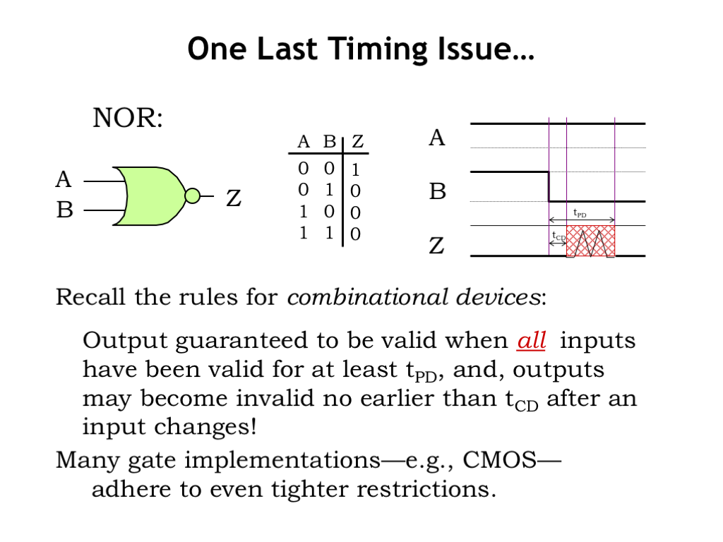
It turns out we can say a bit more about the timing of output transitions for CMOS logic gates. Let’s start by considering the behavior of a non-CMOS combinational device that implements the NOR function. Looking at the waveform diagram, we see that initially the A and B inputs are both 0, and the output Z is 1, just as specified by the truth table. Now B makes a 0-to-1 transition and the Z output will eventually reflect that change by making a 1-to-0 transition. As we learned in the previous video, the timing of the Z transition is determined by the contamination and propagation delays of the NOR gate. Note that we can’t say anything about the value of the Z output in the interval of \(t_{\textrm{CD}}\) to \(t_{\textrm{PD}}\) after the input transition, which we indicate with a red shaded region on the waveform diagram.
Now, let’s consider a different set up, where initially both A and B are 1, and, appropriately, the output Z is 0. Examining the truth table we see that if A is 1, the output Z will be 0 regardless of the value of B. So what happens when B makes a 1-to-0 transition? Before the transition, Z was 0 and we expect it to be 0 again, \(t_{\textrm{PD}}\) after the B transition. But, in general, we can’t assume anything about the value of Z in the interval between \(t_{\textrm{CD}}\) and \(t_{\textrm{PD}}\). Z could have any behavior it wants in that interval and the device would still be a legitimate combinational device.
Many gate technologies — e.g., CMOS — adhere to even tighter restrictions.
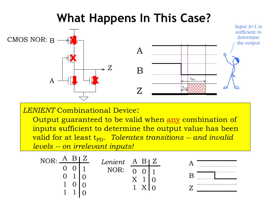
Let’s look in detail at the switch configuration in a CMOS implementation of a NOR gate when both inputs are a digital 1. A high gate voltage will turn on NFET switches (as indicated by the red arrows) and turn off PFET switches (as indicated by the red X’s). Since the pullup circuit is not conducting and the pulldown circuit is conducting, the output Z is connected to GND, the voltage for a digital 0 output.
Now, what happens when the B input transitions from 1 to 0? The switches controlled by B change their configuration: the PFET switch is now on and the NFET switch is now off. But overall the pullup circuit is still not conducting and there is still a pulldown path from Z to GND. So while there used to be two paths from Z to GND and there is now only one path, Z has been connected to GND the whole time and its value has remained valid and stable throughout B’s transition. In the case of a CMOS NOR gate, when one input is a digital 1, the output will be unaffected by transitions on the other input.
A lenient combinational device is one that exhibits this behavior, namely that the output is guaranteed to be be valid when any combination of inputs sufficient to determine the output value has been valid for at least \(t_{\textrm{PD}}\). When some of the inputs are in a configuration that triggers this lenient behavior, transitions on the other inputs will have no effect on the validity of the output value. Happily most CMOS implementations of logic gates are naturally lenient.
We can extend our truth-table notation to indicate lenient behavior by using X for the input values on certain rows to indicate that input value is irrelevant when determining the correct output value. The truth table for a lenient NOR gate calls out two such situations: when A is 1, the value of B is irrelevant, and when B is 1, the value of A is irrelevant. Transitions on the irrelevant inputs don’t trigger the \(t_{\textrm{CD}}\) and \(t_{\textrm{PD}}\) output timing normally associated with an input transition.
When does lenience matter? We’ll need lenient components when building memory components, a topic we’ll get to in a couple of lectures.
You’re ready to try building some CMOS gates of your own!