L05: Sequential Logic
- Something We Can’t Build (Yet)
- Digital State: What We’d Like to Build
- Memory: Using Capacitors
- Memory: Using Feedback
- Settable Memory Element
- New Device: D Latch
- A Plea for Lenience
- … With a Little Discipline
- Let’s Try it Out!
- Flakey Control Systems
- Solution: Escapement Strategy (2 Gates)
- Edge-triggered D Register
- D-Register Waveforms
- Um, About That Hold Time…
- D-Register Timing
- Single-clock Synchronous Circuits
- Timing in a Single-clock System
- Model: Discrete Time
- Sequential Circuit Timing
- Summary
Content of the following slides is described in the surrounding text.
In the last lecture we learned how to build combinational logic circuits given a functional specification that told us how output values were related to the current values of the inputs.
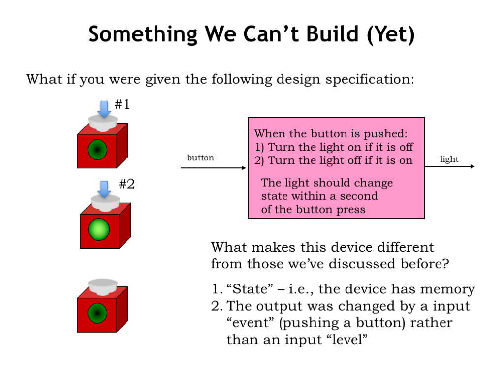
But here’s a simple device we can’t build with combinational logic. The device has a light that serves as the output and push button that serves as the input. If the light is off and we push the button, the light turns on. If the light is on and we push the button, the light turns off.
What makes this circuit different from the combinational circuits we’ve discussed so far? The biggest difference is that the device’s output is not function of the device’s *current* input value. The behavior when the button is pushed depends on what has happened in the past: odd numbered pushes turn the light on, even numbered pushes turn the light off. The device is “remembering” whether the last push was an odd push or an even push so it will behave according to the specification when the next button push comes along. Devices that remember something about the history of their inputs are said to have state.
The second difference is more subtle. The push of the button marks an event in time: we speak of the state before the push (“the light is on”) and state after the push (“the light is off”). It’s the transition of the button from un-pushed to pushed that we’re interested in, not the whether the button is currently pushed or not.
The device’s internal state is what allows it to produce different outputs even though it receives the same input. A combinational device can’t exhibit this behavior since its outputs depends only on the current values of the input. Let’s see how we’ll incorporate the notion of device state into our circuitry.
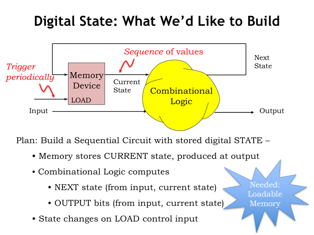
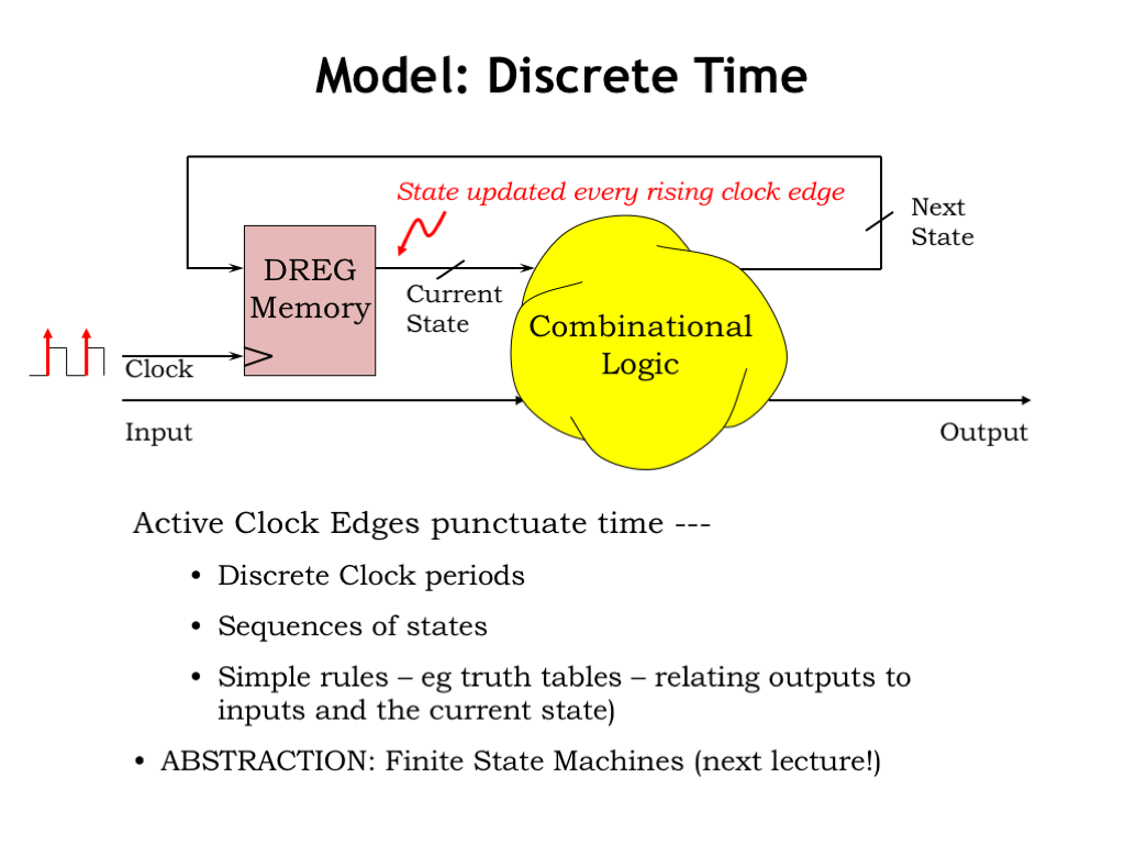
We’ll introduce a new abstraction of a memory component that will store the current state of the digital system we want to build. The memory component stores one or more bits that encode the current state of the system. These bits are available as digital values on the memory component’s outputs, shown here as the wire marked “Current State”.
The current state, along with the current input values, are the inputs to a block of combinational logic that produces two sets of outputs. One set of outputs is the next state of the device, encoded using the same number of bits as the current state. The other set of outputs are the signals that serve as the outputs of the digital system. The functional specification for the combinational logic (perhaps a truth table, or maybe a set of Boolean equations) specifies how the next state and system outputs are related to the current state and current inputs.
The memory component has two inputs: a LOAD control signal that indicates when to replace the current state with the next state, and a data input that specifies what the next state should be. Our plan is to periodically trigger the LOAD control, which will produce a sequence of values for the current state. Each state in the sequence is determined from the previous state and the inputs at the time the LOAD was triggered.
Circuits that include both combinational logic and memory components are called sequential logic. The memory component has a specific capacity measured in bits. If the memory component stores K bits, that puts an upper bound of \(2^K\) on the number of possible states since the state of the device is encoded using the K bits of memory.
So, we’ll need to figure out how to build a memory component that can loaded with new values now and then. That’s the subject of this chapter. We’ll also need a systematic way of designing sequential logic to achieve the desired sequence of actions. That’s the subject of the next chapter.
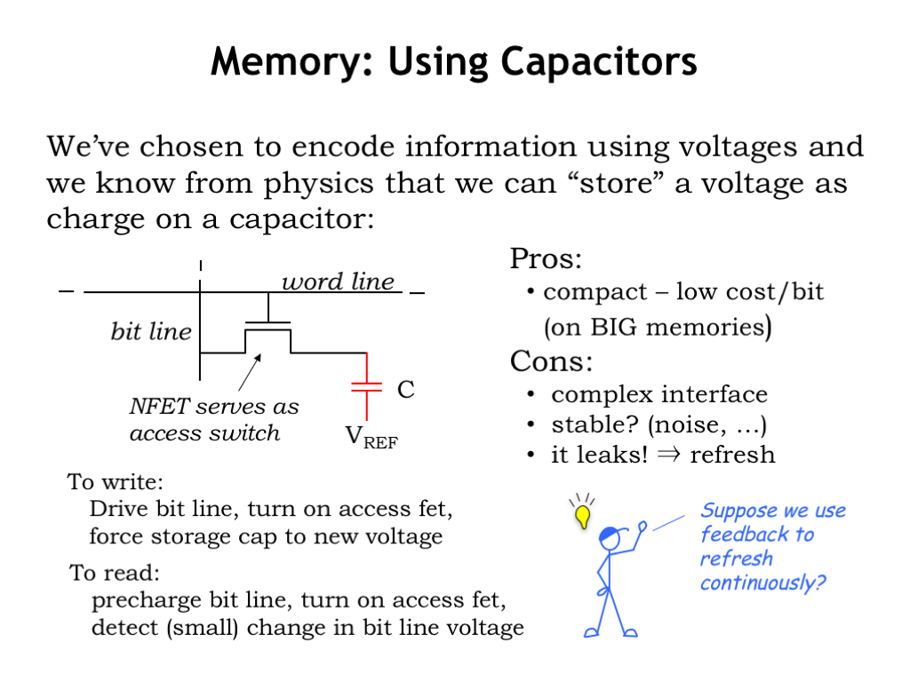
We’ve been representing bits as voltages, so we might consider using a capacitor to store a particular voltage. The capacitor is passive two-terminal device. The terminals are connected to parallel conducting plates separated by insulator. Adding charge Q to one plate of the capacitor generates a voltage difference V between the two plate terminals. Q and V are related by the capacitance C of the capacitor: Q = CV.
When we add charge to a capacitor by hooking a plate terminal to higher voltage, that’s called “charging the capacitor”. And when we take away charge by connecting the plate terminal to a lower voltage, that’s called “discharging the capacitor”.
So here’s how a capacitor-based memory device might work. One terminal of the capacitor is hooked to some stable reference voltage. We’ll use an NFET switch to connect the other plate of the capacitor to a wire called the bit line. The gate of the NFET switch is connected to a wire called the word line.
To write a bit of information into our memory device, drive the bit line to the desired voltage (i.e., a digital 0 or a digital 1). Then set the word line HIGH, turning on the NFET switch. The capacitor will then charge or discharge until it has the same voltage as the bit line. At this point, set the word line LOW, turning off the NFET switch and isolating the capacitor’s charge on the internal plate. In a perfect world, the charge would remain on the capacitor’s plate indefinitely.
At some later time, to access the stored information, we first charge the bit line to some intermediate voltage. Then set the word line HIGH, turning on the NFET switch, which connects the charge on the bit line to the charge on the capacitor. The charge sharing between the bit line and capacitor will have some small effect on the charge on the bit line and hence its voltage. If the capacitor was storing a digital 1 and hence was at a higher voltage, charge will flow from the capacitor into the bit line, raising the voltage of the bit line. If the capacitor was storing a digital 0 and was at lower voltage, charge will flow from the bit line into the capacitor, lowering the voltage of the bit line. The change in the bit line’s voltage depends on the ratio of the bit line capacitance to C, the storage capacitor’s capacitance, but is usually quite small. A very sensitive amplifier, called a sense amp, is used to detect that small change and produce a legal digital voltage as the value read from the memory cell.
Whew! Reading and writing require a whole sequence of operations, along with carefully designed analog electronics. The good news is that the individual storage capacitors are quite small — in modern integrated circuits we can fit billions of bits of storage on relatively inexpensive chips called dynamic random-access memories, or DRAMs for short. DRAMs have a very low cost per bit of storage.
The bad news is that the complex sequence of operations required for reading and writing takes a while, so access times are relatively slow. And we have to worry about carefully maintaining the charge on the storage capacitor in the face of external electrical noise. The really bad news is that the NFET switch isn’t perfect and there’s a tiny amount leakage current across the switch even when it’s officially off. Over time that leakage current can have a noticeable impact on the stored charge, so we have to periodically refresh the memory by reading and re-writing the stored value before the leakage has corrupted the stored information. In current technologies, this has to be done every 10ms or so.
Hmm. Maybe we can get around the drawbacks of capacitive storage by designing a circuit that uses feedback to provide a continual refresh of the stored information…
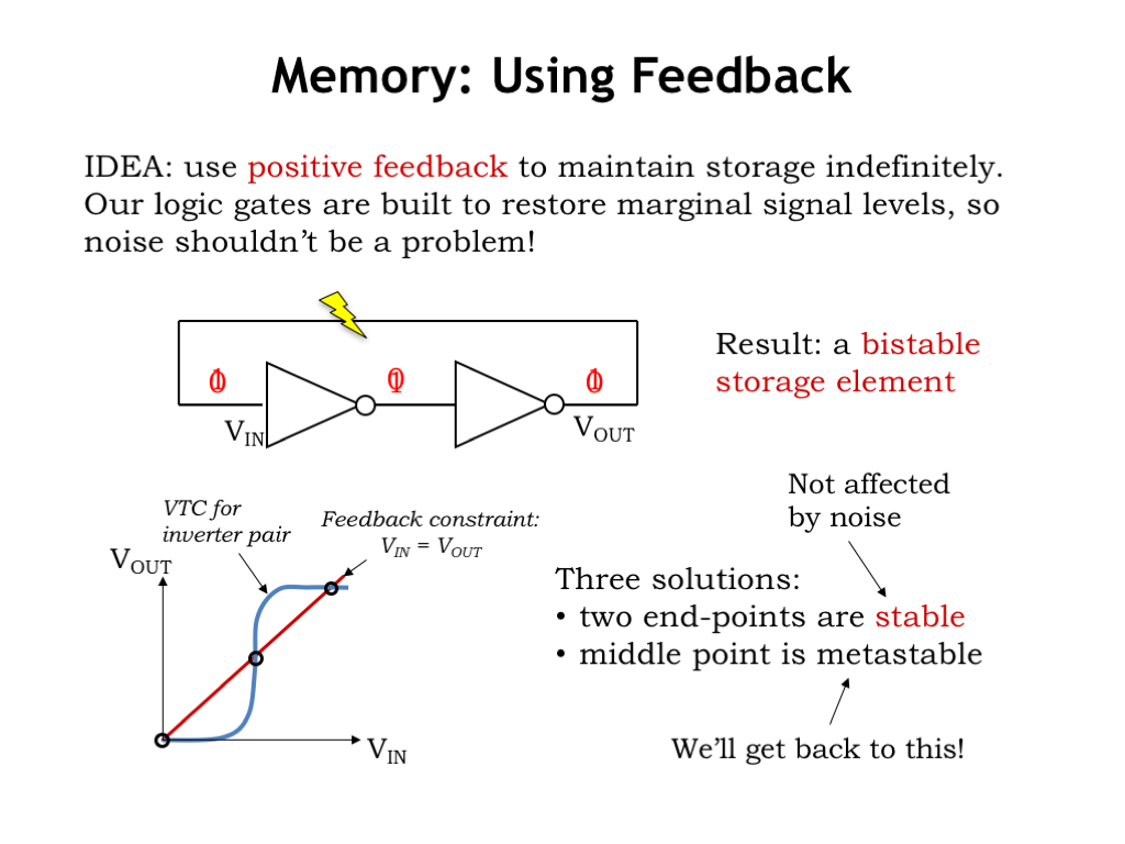
Here’s a circuit using combinational inverters hooked in a positive feedback loop. If we set the input of one of the inverters to a digital 0, it will produce a digital 1 on its output. The second inverter will then a produce a digital 0 on its output, which is connected back around to the original input. This is a stable system and these digital values will be maintained, even in the presence of noise, as long as this circuitry is connected to power and ground. And, of course, it’s also stable if we flip the digital values on the two wires. The result is a system that has two stable configurations, called a bi-stable storage element.
Here’s the voltage transfer characteristic showing how \(V_{\textrm{OUT}}\) and \(V_{\textrm{IN}}\) of the two-inverter system are related. The effect of connecting the system’s output to its input is shown by the added constraint that \(V_{\textrm{IN}}\) equal \(V_{\textrm{OUT}}\). We can then graphically solve for values of \(V_{\textrm{IN}}\) and \(V_{\textrm{OUT}}\) that satisfy both constraints. There are three possible solutions where the two curves intersect.
The two points of intersection at either end of the VTC are stable in the sense that small changes in \(V_{\textrm{IN}}\) (due, say, to electrical noise), have no effect on \(V_{\textrm{OUT}}\). So the system will return to its stable state despite small perturbations.
The middle point of intersection is what we call metastable. In theory the system could “balance” at this particular \(V_{\textrm{IN}}/V_{\textrm{OUT}}\) voltage forever, but the smallest perturbation will cause the voltages to quickly transition to one of the stable solutions. Since we’re planing to use this bi-stable storage element as our memory component, we’ll need to figure out how to avoid getting the system into this metastable state. More on this in the next chapter.
Now let’s figure out how to load new values into our bi-stable storage element.
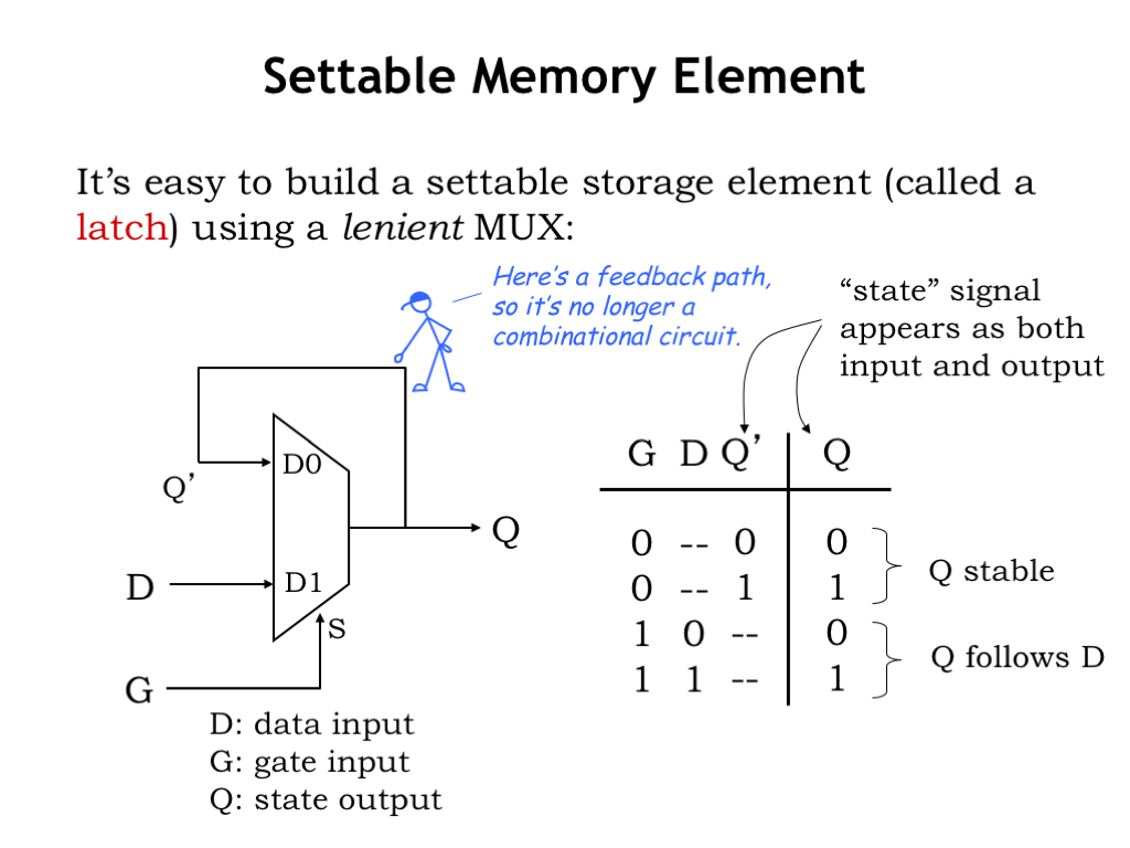
We can use a 2-to-1 multiplexer to build a settable storage element. Recall that a MUX selects as its output value the value of one of its two data inputs. The output of the MUX serves as the state output of the memory component. Internally to the memory component we’ll also connect the output of the MUX to its D0 data input. The MUX{}’s D1 data input will become the data input of the memory component. And the select line of the MUX will become the memory component’s load signal, here called the gate.
When the gate input is LOW, the MUX{}’s output is looped back through MUX through the D0 data input, forming the bi-stable positive feedback loop discussed in the last section. Note our circuit now has a cycle, so it no longer qualifies as a combinational circuit.
When the gate input is HIGH, the MUX{}’s output is determined by the value of the D1 input, i.e., the data input of the memory component.
To load new data into the memory component, we set the gate input HIGH for long enough for the Q output to become valid and stable. Looking at the truth table, we see that when G is 1, the Q output follows the D input. While the G input is HIGH, any changes in the D input will be reflected as changes in the Q output, the timing being determined by the tPD of the MUX.
Then we can set the gate input LOW to switch the memory component into memory mode, where the stable Q value is maintained indefinitely by the positive feedback loop as shown in the first two rows of the truth table.
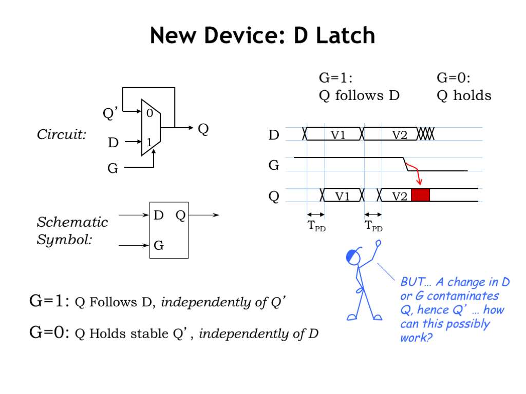
Our memory device is a called a D latch, or just a latch for short, with the schematic symbol shown here.
When the latch’s gate is HIGH, the latch is open and information flows from the D input to the Q output. When the latch’s gate is LOW, the latch is closed and in “memory mode”, remembering whatever value was on the D input when the gate transitioned from HIGH to LOW.
This is shown in the timing diagrams on the right. The waveforms show when a signal is stable, i.e., a constant signal that’s either LOW or HIGH, and when a signal is changing, shown as one or more transitions between LOW and HIGH.
When G is HIGH, we can see Q changing to a new stable output value no later than tPD after D reaches a new stable value.
Our theory is that after G transitions to a LOW value, Q will stay stable at whatever value was on D when G made the HIGH to LOW transition. But, we know that in general, we can’t assume anything about the output of a combinational device until tPD after the input transition — the device is allowed to do whatever it wants in the interval between tCD and tPD after the input transition. But how will our memory work if the 1-to-0 transition on G causes the Q output to become invalid for a brief interval? After all it’s the value on the Q output we’re trying to remember! We’re going to have ensure that a 1-to-0 transition on G doesn’t affect the Q output.
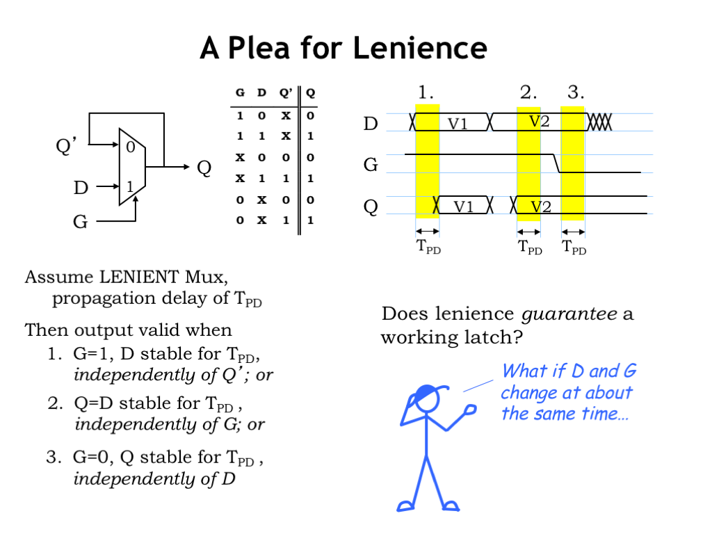
That’s why we specified a lenient MUX for our memory component. The truth table for a lenient MUX is shown here. The output of a lenient MUX remains valid and stable even after an input transition under any of the following three conditions.
(1) When we’re loading the latch by setting G HIGH, once the D input has been valid and stable for tPD, we are guaranteed that the Q output will be stable and valid with the same value as the D input, independently of Q’s initial value.
Or (2) If both Q and D are valid and stable for tPD, the Q output will be unaffected by subsequent transitions on the G input. This is the situation that will allow us to have a 1-to-0 transition on G without contaminating the Q output.
Or, finally, (3) if G is LOW and Q has been stable for at least tPD, the output will be unaffected by subsequent transitions on the D input.
Does lenience guarantee a working latch? Well, only if we’re careful about ensuring that signals are stable at the right times so we can leverage the lenient behavior of the MUX.
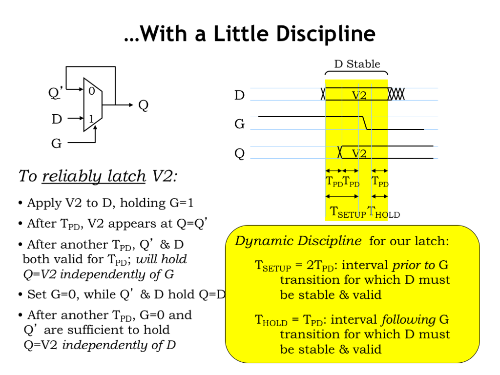
Here are the steps we need to follow in order to ensure the latch will work as we want.
First, while the G input is HIGH, set the D input to the value we wish store in the latch. Then, after tPD, we’re guaranteed that value will be stable and valid on the Q output. This is condition (1) from the previous slide.
Now we wait another tPD so that the information about the new value on the Q’ input propagates through the internal circuitry of the latch. Now, both D *and* Q’ have been stable for at least tPD, giving us condition (2) from the previous slide.
So if D is stable for 2*tPD, transitions on G will not affect the Q output. This requirement on D is called the setup time of the latch: it’s how long D must be stable and valid before the HIGH-to-LOW transition of G.
Now we can set G to LOW, still holding D stable and valid. After another tPD to allow the new G value to propagate through the internal circuitry of the latch, we’ve satisfied condition (3) from the previous slide, and the Q output will be unaffected by subsequent transitions on D.
This further requirement on D’s stability is called the hold time of the latch: it’s how long after the transition on G that D must stay stable and valid.
Together the setup and hold time requirements are called the dynamic discipline, which must be followed if the latch is to operate correctly.
In summary, the dynamic discipline requires that the D input be stable and valid both both before and after a transition on G. If our circuit is designed to obey the dynamic discipline, we can guarantee that this memory component will reliably store the information on D when the gate makes a HIGH-to-LOW transition.
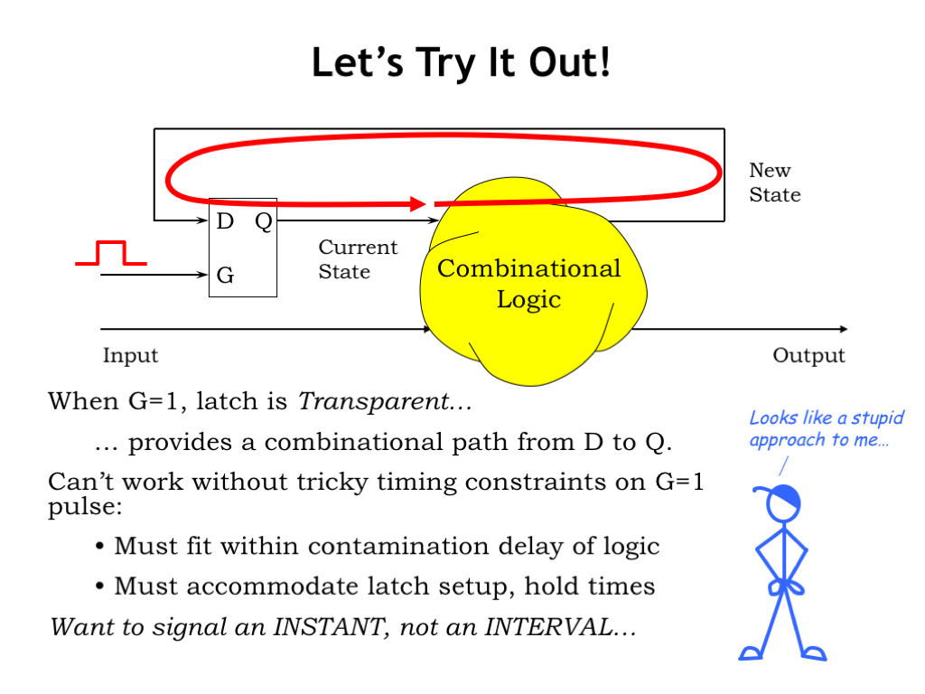
Let’s try using the latch as the memory component in our sequential logic system.
To load the encoding of the new state into the latch, we open the latch by setting the latch’s gate input HIGH, letting the new value propagate to the latch’s Q output, which represents the current state. This updated value propagates through the combinational logic, updating the new state information. Oops, if the gate stays HIGH too long, we’ve created a loop in our system and our plan to load the latch with new state goes awry as the new state value starts to change rapidly as information propagates around and around the loop.
So to make this work, we need to carefully time the interval when G is HIGH. It has to be long enough to satisfy the constraints of the dynamic discipline, but it has to be short enough that the latch closes again before the new state information has a chance to propagate all the way around the loop.
Hmm. I think Mr. Blue is right: this sort of tricky system timing would likely be error-prone since the exact timing of signals is almost impossible to guarantee. We have upper and lower bounds on the timing of signal transitions but no guarantees of exact intervals. To make this work, we want to a load signal that marks an instant in time, not an interval.
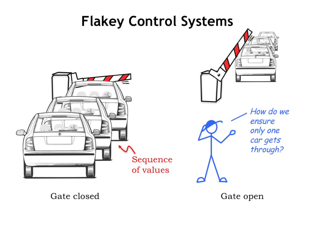
Here’s an analogy that will help us understand what’s happening and what we can do about it. Imagine a line cars waiting at a toll booth gate. The sequence of cars represents the sequence of states in our sequential logic and the gated toll both represents the latch.
Initially the gate is closed and the cars are waiting patiently to go through the toll booth. When the gate opens, the first car proceeds out of the toll both. But you can see that the timing of when to close the gate is going to be tricky. It has to be open long enough for the first car to make it through, but not too long lest the other cars also make it through. This is exactly the issue we faced with using the latch as our memory component in our sequential logic.
So how do we ensure only one car makes it through the open gate?
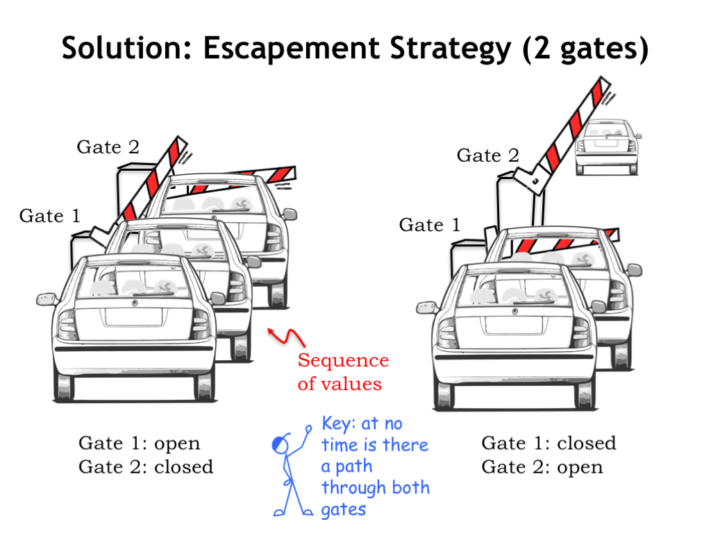
One solution is to use two gates! Here’s the plan: Initially Gate 1 is open allowing exactly one car to enter the toll booth and Gate 2 is closed. Then at a particular point in time, we close Gate 1 while opening Gate 2. This lets the car in the toll booth proceed on, but prevents any other car from passing through. We can repeat this two-step process to deal with each car one-at-time. The key is that at no time is there a path through both gates.
This is the same arrangement as the escapement mechanism in a mechanical clock. The escapement ensures that the gear attached to the clock’s spring only advances one tooth at a time, preventing the spring from spinning the gear wildly causing a whole day to pass at once!
If we observed the toll booth’s output, we would see a car emerge shortly after the instant in time when Gate 2 opens. The next car would emerge shortly after the next time Gate 2 opens, and so on. Cars would proceed through the toll booth at a rate set by the interval between Gate 2 openings.
Let’s apply this solution to design a memory component for our sequential logic.
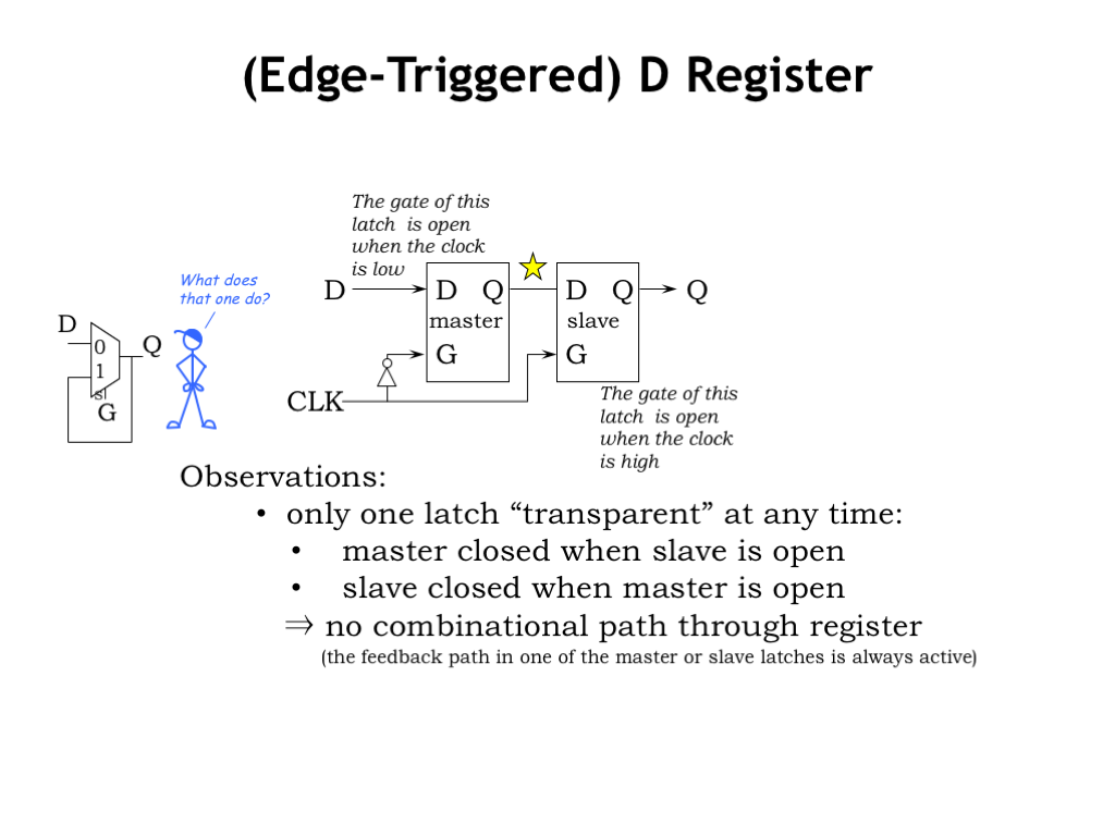
Taking our cue from the 2-gate toll both, we’ll design a new component, called a D register, using two back-to-back latches. The load signal for a D register is typically called the register’s “clock”, but the register’s D input and Q output play the same roles as they did for the latch.
First we’ll describe the internal structure of the D register, then we’ll describe what it does and look in detail at how it does it.
The D input is connected to what we call the master latch and the Q output is connected to the slave latch.
Note that the clock signal is inverted before it’s connected to the gate input of the master latch. So when the master latch is open, the slave is closed, and vice versa. This achieves the escapement behavior we saw on the previous slide: at no time is there active path from the register’s D input to the register’s Q output.
The delay introduced by the inverter on the clock signal might give us cause for concern. When there’s a rising 0-to-1 transition on the clock signal, might there be a brief interval when the gate signal is HIGH for both latches since there will be a small delay before the inverter’s output transitions from 1 to 0? Actually the inverter isn’t necessary: Mr Blue is looking at a slightly different latch schematic where the latch is open when G is LOW and closed when G is high. Just what we need for the master latch!
By the way, you’ll sometimes hear a register called a flip-flop because of the bistable nature of the positive feedback loops in the latches.
That’s the internal structure of the D register. In the next section we’ll take a step-by-step tour of the register in operation.
We’ll get a good understanding of how the register operates as we follow the signals through the circuit.
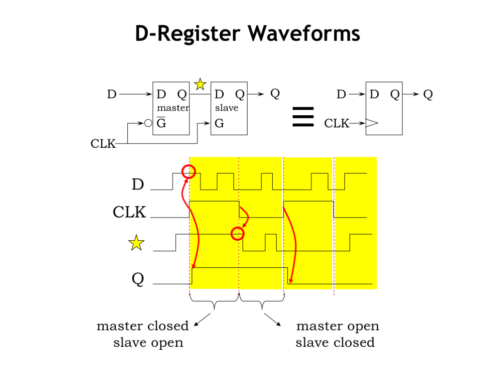
The overall operation of the register is simple: At the rising 0-to-1 transition of the clock input, the register samples the value of the D input and stores that value until the next rising clock edge. The Q output is simply the value stored in the register. Let’s see how the register implements this functionality.
The clock signal is connected to the gate inputs of the master and slave latches. Since all the action happens when the clock makes a transition, it’s those events we’ll focus on. The clock transition from LOW to HIGH is called the rising edge of the clock. And its transition from HIGH to LOW is called the falling edge. Let’s start by looking the operation of the master latch and its output signal, which is labeled STAR in the diagram.
On the rising edge of the clock, the master latch goes from open to closed, sampling the value on its input and entering memory mode. The sampled value thus becomes the output of the latch as long as the latch stays closed. You can see that the STAR signal remains stable whenever the clock signal is high.
On the falling edge of the clock the master latch opens and its output will then reflect any changes in the D input, delayed by the tPD of the latch.
Now let’s figure out what the slave is doing. It’s output signal, which also serves as the output of D register, is shown as the bottom waveform. On the rising edge of the clock the slave latch opens and its output will follow the value of the STAR signal. Remember though that the STAR signal is stable while the clock is HIGH since the master latch is closed, so the Q signal is also stable after an initial transition if value saved in the slave latch is changing.
At the falling clock edge [CLICK], the slave goes from open to closed, sampling the value on its input and entering memory mode. The sampled value then becomes the output of the slave latch as long as the latch stays closed. You can see that that the Q output remains stable whenever the clock signal is LOW.
Now let’s just look at the Q signal by itself for a moment. It only changes when the slave latch opens at the rising edge of the clock. The rest of the time either the input to slave latch is stable or the slave latch is closed. The change in the Q output is triggered by the rising edge of the clock, hence the name “positive-edge-triggered D register”.
The convention for labeling the clock input in the schematic icon for an edge-triggered device is to use a little triangle. You can see that here in the schematic symbol for the D register.
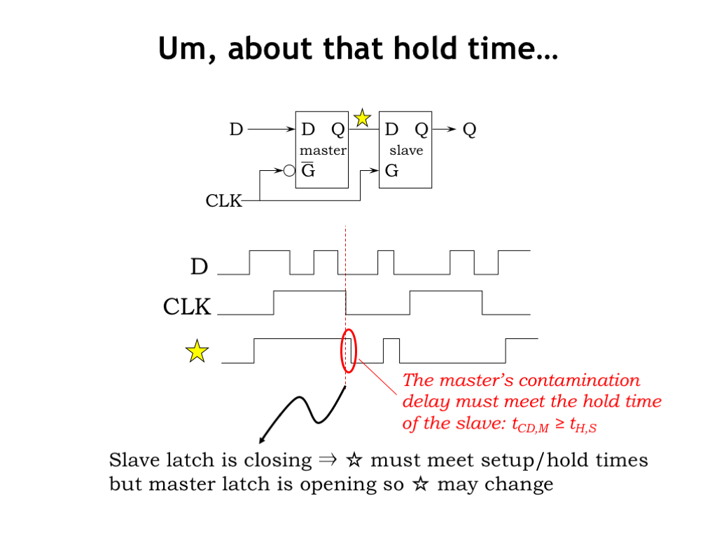
There is one tricky problem we have to solve when designing the circuitry for the register. On the falling clock edge, the slave latch transitions from open to closed and so its input (the STAR signal) must meet the setup and hold times of the slave latch in order to ensure correct operation.
The complication is that the master latch opens at the same time, so the STAR signal may change shortly after the clock edge. The contamination delay of the master latch tells us how long the old value will be stable after the falling clock edge. And the hold time on the slave latch tells us how long it has to remain stable after the falling clock edge.
So to ensure correct operation of the slave latch, the contamination delay of the master latch has to be greater than or equal to the hold time of the slave latch. Doing the necessary analysis can be a bit tricky since we have to consider manufacturing variations as well as environmental factors such as temperature and power supply voltage. If necessary, extra gate delays (e.g., pairs of inverters) can be added between the master and slave latches to increase the contamination delay on the slave’s input relative to the falling clock edge. Note that we can only solve slave latch hold time issues by changing the design of the circuit.
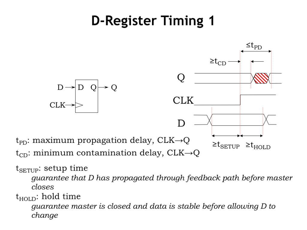
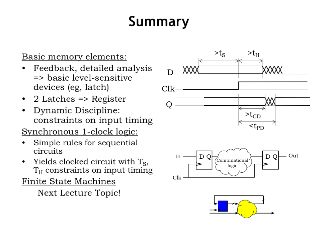
Here’s a summary of the timing specifications for a D register.
Changes in the Q signal are triggered by a rising edge on the clock input. The propagation delay \(t_{\textrm{PD}}\) of the register is an upper bound on the time it takes for the Q output to become valid and stable after the rising clock edge.
The contamination delay of the register is a lower bound on the time the previous value of Q remains valid after the rising clock edge.
Note that both \(t_{\textrm{CD}}\) and \(t_{\textrm{PD}}\) are measured relative to the rising edge of the clock. Registers are designed to be lenient in the sense that if the previous value of Q and the new value of Q are the same, the stability of the Q signal is guaranteed during the rising clock edge. In other words, the \(t_{\textrm{CD}}\) and \(t_{\textrm{PD}}\) specifications only apply when the Q output actually changes.
In order to ensure correct operation of the master latch, the register’s D input must meet the setup and hold time constraints for the master latch. So the following two specifications are determined by the timing of the master latch.
\(t_{\textrm{SETUP}}\) is the amount of time that the D input must be valid and stable before the rising clock edge and \(t_{\textrm{HOLD}}\) is the amount of time that D must be valid and stable after the rising clock. This region of stability surrounding the clock edge ensures that we’re obeying the dynamic discipline for the master latch.
So when you use a D register component from a manufacturer’s gate library, you’ll need to look up these four timing specifications in the register’s data sheet in order to analyze the timing of your overall circuit. We’ll see how this analysis is done in the next section.
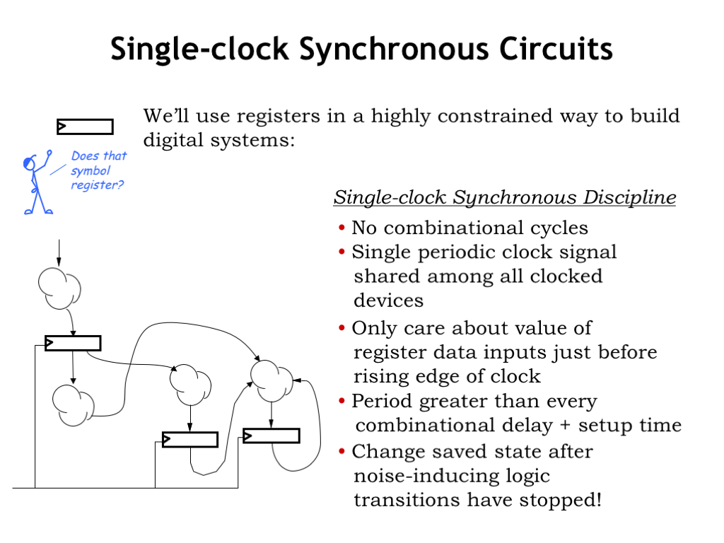
In 6.004, we have a specific plan on how we’ll use registers in our designs, which we call the single-clock synchronous discipline.
Looking at the sketch of a circuit on the left, we see that it consists of registers — the rectangular icons with the edge-triggered symbol — and combinational logic circuits, shown here as little clouds with inputs and outputs.
Remembering that there is no combinational path between a register’s input and output, the overall circuit has no combinational cycles. In other words, paths from system inputs and register outputs to the inputs of registers never visit the same combinational block twice.
A single periodic clock signal is shared among all the clocked devices. Using multiple clock signals is possible, but analyzing the timing for signals that cross between clock domains is quite tricky, so life is much simpler when all registers use the same clock.
The details of which data signals change when are largely unimportant. All that matters is that signals hooked to register inputs are stable and valid for long enough to meet the registers’ setup time. And, of course, stay stable long enough to meet the registers’ hold time.
We can guarantee that the dynamic discipline is obeyed by choosing the clock period to be greater then the \(t_{\textrm{PD}}\) of every path from register outputs to register inputs, plus, of course, the registers’ setup time.
A happy consequence of choosing the clock period in this way is that at the moment of the rising clock edge, there are no other noise-inducing logic transitions happening anywhere in the circuit. Which means there should be no noise problems when we update the stored state of each register.
Our next task is to learn how to analyze the timing of a single-clock synchronous system.
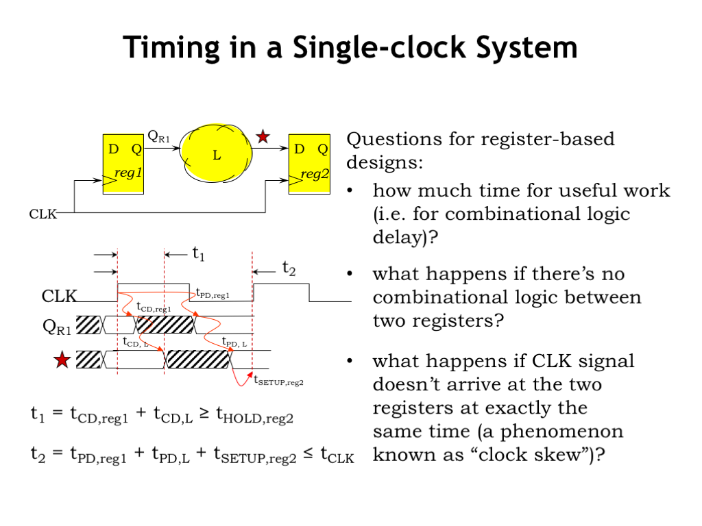
Here’s a model of a particular path in our synchronous system. A large digital system will have many such paths and we have to do the analysis below for each one in order to find the path that will determine the smallest workable clock period. As you might suspect, there are computed-aided design programs that will do these calculations for us.
There’s an upstream register, whose output is connected to a combinational logic circuit which generates the input signal, labeled STAR, to the downstream register.
Let’s build a carefully-drawn timing diagram showing when each signal in the system changes and when it is stable.
The rising edge of the clock triggers the upstream register, whose output (labeled \(Q_{\textsc{r1}}\)) changes as specified by the contamination and propagation delays of the register. \(Q_{\textsc{r1}}\) maintains its old value for at least the contamination delay of REG1, and then reaches its final stable value by the propagation delay of REG1. At this point \(Q_{\textsc{r1}}\) will remain stable until the next rising clock edge.
Now let’s figure out the waveforms for the output of the combinational logic circuit, marked with a red star in the diagram. The contamination delay of the logic determines the earliest time STAR will go invalid measured from when \(Q_{\textsc{r1}}\) went invalid. The propagation delay of the logic determines the latest time STAR will be stable measured from when \(Q_{\textsc{r1}}\) became stable.
Now that we know the timing for STAR, we can determine whether STAR will meet the setup and hold times for the downstream register REG2. Time t1 measures how long STAR will stay valid after the rising clock edge. t1 is the sum of REG1’s contamination delay and the logic’s contamination delay. The HOLD time for REG2 measures how long STAR has to stay valid after the rising clock edge in order to ensure correct operation. So t1 has to be greater than or equal to the HOLD time for REG2.
Time t2 is the sum of the propagation delays for REG1 and the logic, plus the SETUP time for REG2. This tells us the earliest time at which the next rising clock edge can happen and still ensure that the SETUP time for REG2 is met. So t2 has to be less than or equal to the time between rising clock edges, called the clock period or tCLK. If the next rising clock happens before t2, we’ll be violating the dynamic discipline for REG2.
So we have two inequalities that must be satisfied for every register-to-register path in our digital system. If either inequality is violated, we won’t be obeying the dynamic discipline for REG2 and our circuit will not be guaranteed to work correctly.
Looking at the inequality involving tCLK, we see that the propagation delay of the upstream register and setup time for the downstream register take away from the time available useful work performed by the combinational logic. Not surprisingly, designers try to use registers that minimize these two times.
What happens if there’s no combinational logic between the upstream and downstream registers? This happens when designing shift registers, digital delay lines, etc. Well, then the first inequality tells us that the contamination delay of the upstream register had better be greater than or equal to the hold time of the downstream register. In practice, contamination delays are smaller than hold times, so in general this wouldn’t be the case. So designers are often required to insert dummy logic, e.g., two inverters in series, in order to create the necessary contamination delay.
Finally we have to worry about the phenomenon called clock skew, where the clock signal arrives at one register before it arrives at the other. We won’t go into the analysis here, but the net effect is to increase the apparent setup and hold times of the downstream register, assuming we can’t predict the sign of the skew.
The clock period, tCLK, characterizes the performance of our system. You may have noticed that Intel is willing to sell you processor chips that run at different clock frequencies, e.g., a 1.7 GHz processor vs. a 2 GHz processor. Did you ever wonder how those chips are different? As is turns out they’re not! What’s going on is that variations in the manufacturing process mean that some chips have better tPDs than others. On fast chips, a smaller tPD for the logic means that they can have a smaller tCLK and hence a higher clock frequency. So Intel manufactures many copies of the same chip, measures their tPDs and selects the fast ones to sell as higher-performance parts. That’s what it takes to make money in the chip biz!
Using a D register as the memory component in our sequential logic system works great! At each rising edge of the clock, the register loads the new state, which then appears at the register’s output as the current state for the rest of the clock period. The combinational logic uses the current state and the value of the inputs to calculate the next state and the values for the outputs. A sequence of rising clock edges and inputs will produce a sequence of states, which leads to a sequence of outputs. In the next chapter we’ll introduce a new abstraction, finite state machines, that will make it easy to design sequential logic systems.
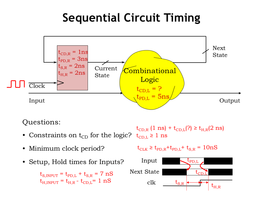
Let’s use the timing analysis techniques we’ve learned on the sequential logic system shown here. The timing specifications for the register and combinational logic are as shown. Here are the questions we need to answer.
The contamination delay of the combinational logic isn’t specified. What does it have to be in order for the system to work correctly? Well, we know that the sum of register and logic contamination delays has to be greater than or equal to the hold time of the register. Using the timing parameters we do know along with a little arithmetic tells us that the contamination delay of the logic has to be at least 1 ns.
What is the minimum value for the clock period tCLK? The second timing inequality from the previous section tells us that tCLK has be greater than than the sum of the register and logic propagation delays plus the setup time of the register. Using the known values for these parameters gives us a minimum clock period of 10ns.
What are the timing constraints for the Input signal relative to the rising edge of the clock? For this we’ll need a diagram! The Next State signal is the input to the register so it has to meet the setup and hold times as shown here. Next we show the Input signal and how the timing of its transitions affect to the timing of the Next State signal. Now it’s pretty easy to figure out when Input has to be stable before the rising edge of the clock, i.e., the setup time for Input. The setup time for Input is the sum of propagation delay of the logic plus the setup time for the register, which we calculate as 7ns. In other words, if the Input signal is stable at least 7ns before the rising clock edge, then Next State will be stable at least 2ns before the rising clock edge and hence meet the register’s specified setup time.
Similarly, the hold time of Input has to be the hold time of the register minus the contamination delay of the logic, which we calculate as 1 ns. In other words, if Input is stable at least 1 ns after the rising clock edge, then Next State will be stable for another 1 ns, i.e., a total of 2 ns after the rising clock edge. This meets the specified hold time of the register.
This completes our introduction to sequential logic. Pretty much every digital system out there is a sequential logic system and hence is obeying the timing constraints imposed by the dynamic discipline. So next time you see an ad for a 1.7 GHz processor chip, you’ll know where the “1.7” came from!