
L08: Design Tradeoffs
- Optimizing Your Design
- CMOS Static Power Dissipation
- CMOS Dynamic Power Dissipation I
- CMOS Dynamic Power Dissipation II
- How Can We Reduce Power?
- Fewer Transitions → Lower Power
- Improving Speed: Adder Example
- Performance/Cost Analysis
- Carry-Select Adders
- 32-Bit Carry-Select Adder
- Wanted: Faster Carry Logic!
- Carry Look-Ahead Adders (CLA)
- 8-Bit CLA (generate G & P)
- 8-Bit CLA (carry generation)
- 8-Bit CLA (complete)
- Binary Multiplication
- Combinational Multiplier
- 2’s Complement Multiplication
- 2’s Complement Multiplier
- Increase Throughput with Pipelining
- Carry-Save Pipelined Multiplier
- Reduce Area with Sequential Logic
- Summary
Content of the following slides is described in the surrounding text.
In this lecture, we’re going to look into optimizing digital systems to make them smaller, faster, higher performance, more energy efficient, and so on. It would be wonderful if we could achieve all these goals at the same time and for some circuits we can. But, in general, optimizing in one dimension usually means doing less well in another. In other words, there are design tradeoffs to be made.
Making tradeoffs correctly requires that we have a clear understanding of our design goals for the system. Consider two different design teams: one is charged with building a high-end graphics card for gaming, the other with building the Apple watch.
The team building the graphics card is mostly concerned with performance and, within limits, is willing to trade off cost and power consumption to achieve their performance goals. Graphics cards have a set size, so there’s a high priority in making the system small enough to meet the required size, but there’s little to be gained in making it smaller than that.
The team building the watch has very different goals. Size and power consumption are critical since it has to fit on a wrist and run all day without leaving scorch marks on the wearer’s wrist!
Suppose both teams are thinking about pipelining part of their logic for increased performance. Pipelining registers are an obvious additional cost. The overlapped execution and higher \(t_{\textrm{CLK}}\) made possible by pipelining would increase the power consumption and the need to dissipate that power somehow. You can imagine the two teams might come to very different conclusions about the correct course of action!
This chapter takes a look at some of the possible tradeoffs. But as designers you’ll have to pick and choose which tradeoffs are right for your design. This is the sort of design challenge on which good engineers thrive! Nothing is more satisfying than delivering more than anyone thought possible within the specified constraints.
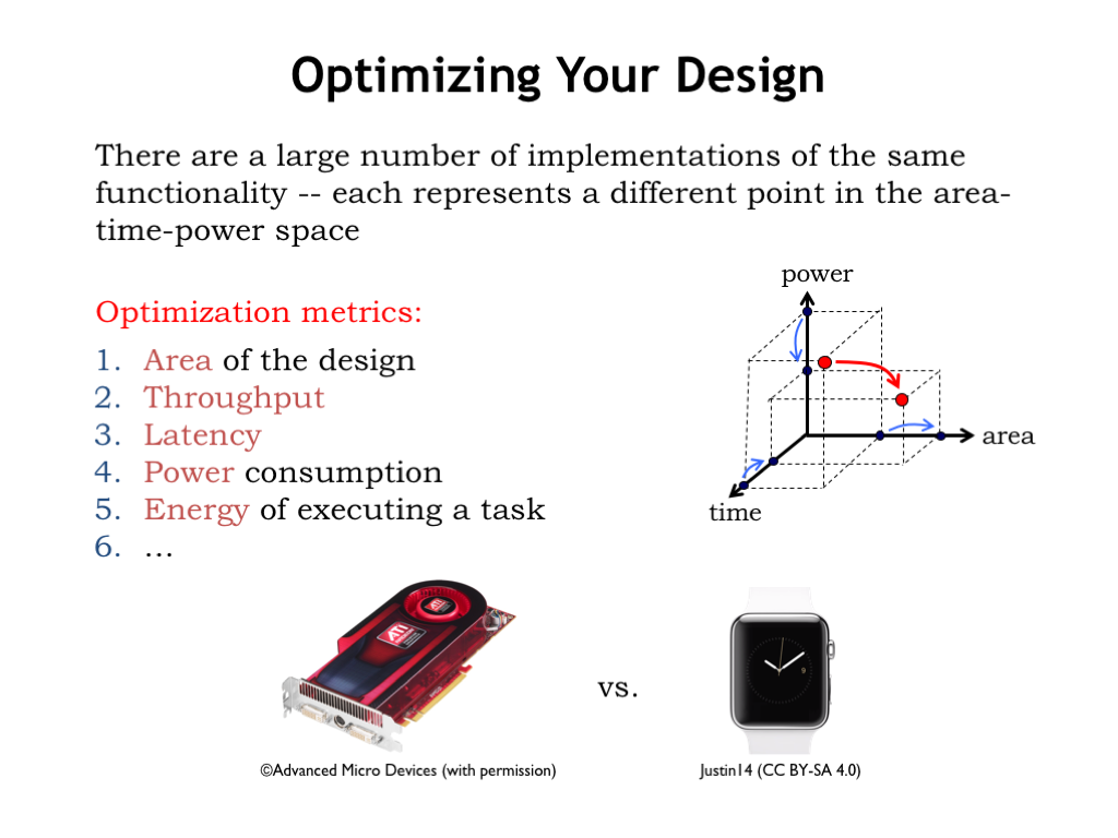
Our first optimization topic is power dissipation, where the usual goal is to either meet a certain power budget, or to minimize power consumption while meeting all the other design targets.
In CMOS circuits, there are several sources of power dissipation, some under our control, some not.
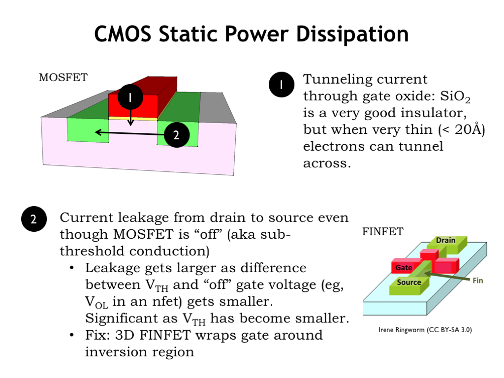
Static power dissipation is power that is consumed even when the circuit is idle, i.e., no nodes are changing value. Using our simple switch model for the operation of MOSFETs, we’d expect CMOS circuits to have zero static power dissipation. And in the early days of CMOS, we came pretty close to meeting that ideal. But as the physical dimensions of the MOSFET have shrunk and the operating voltages have been lowered, there are two sources of static power dissipation in MOSFETs that have begun to loom large.
We’ll discuss the effects as they appear in n-channel MOSFETs, but keep in mind that they appear in p-channel MOSFETs too.
The first effect depends on the thickness of the MOSFET’s gate oxide, shown as the thin yellow layer in the MOSFET diagram on the left. In each new generation of integrated circuit technology, the thickness of this layer has shrunk, as part of the general reduction in all the physical dimensions. The thinner insulating layer means stronger electrical fields that cause a deeper inversion layer that leads to NFETs that carry more current, producing faster gate speeds. Unfortunately the layers are now thin enough that electrons can tunnel through the insulator, creating a small flow of current from the gate to the substrate. With billions of NFETs in a single circuit, even tiny currents can add up to non-negligible power drain.
The second effect is caused by current flowing between the drain and source of a NFET that is, in theory, not conducting because \(V_{\textrm{GS}}\) is less than the threshold voltage. Appropriately this effect is called sub-threshold conduction and is exponentially related to \(V_{\textrm{GS}}\) - \(V_{\textrm{TH}}\) (a negative value when the NFET is off). So as \(V_{\textrm{TH}}\) has been reduced in each new generation of technology, \(V_{\textrm{GS}} - V_{\textrm{TH}}\) is less negative and the sub-threshold conduction has increased.
One fix has been to change the geometry of the NFET so the conducting channel is a tall, narrow fin with the gate terminal wrapped around 3 sides, sometimes referred to as a tri-gate configuration. This has reduced the sub-threshold conduction by an order of magnitude or more, solving this particular problem for now.
Neither of these effects is under the control of the system designer, except of course, if they’re free to choose an older manufacturing process! We mention them here so that you’re aware that newer technologies often bring additional costs that then become part of the trade-off process.
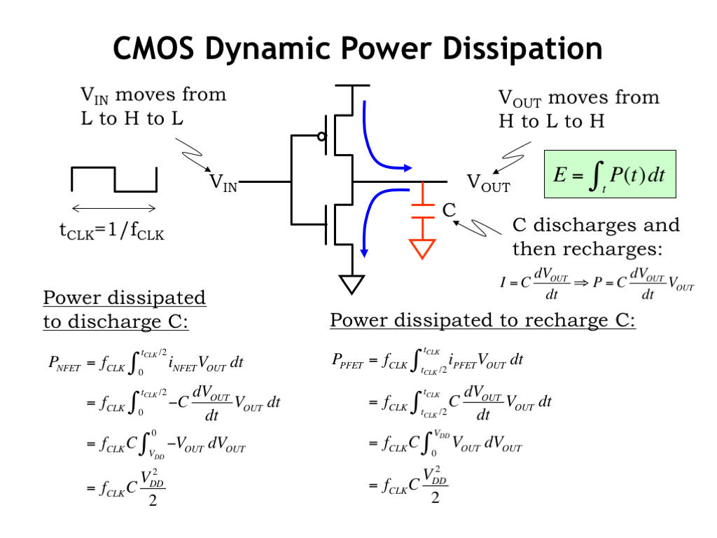
A designer does have some control over the dynamic power dissipation of the circuit, the amount of power spent causing nodes to change value during a sequence of computations. Each time a node changes from 0-to-1 or 1-to-0, currents flow through the MOSFET pullup and pulldown networks, charging and discharging the output node’s capacitance and thus changing its voltage.
Consider the operation of an inverter. As the voltage of the input changes, the pullup and pulldown networks turn on and off, connecting the inverter’s output node to VDD or ground. This charges or discharges the capacitance of the output node changing its voltage. We can compute the energy dissipated by integrating the instantaneous power associated with the current flow through the pullups and pulldowns over the time taken by the output transition.
The power dissipated across the resistance of the MOSFET channel is simply \(I_{\textrm{DS}}\) times \(V_{\textrm{DS}}\). Here’s the energy integral for the 1-to-0 transition of the output node, where we’re measuring \(I_{\textrm{DS}}\) using the equation for the current flowing out of the output node’s capacitor: \(I = C dV/dt\). Assuming that the input signal is a clock signal of period \(t_{\textrm{CLK}}\) and that each transition is taking half a clock cycle, we can work through the math to determine that energy dissipated through the pulldown network is \(0.5 f C V_{\textrm{DD}}^2\), where the frequency \(f\) tells us the number of such transitions per second, \(C\) is the nodal capacitance, and \(V_{\textrm{DD}}\) (the power supply voltage) is the starting voltage of the nodal capacitor.
There’s a similar integral for the current dissipated by the pullup network when charging the capacitor and it yields the same result.
So one complete cycle of charging then discharging dissipates \(f C V^2\) joules. Note that all this energy has come from the power supply — the first half is dissipated when the output node is charged and the other half stored as energy in the capacitor. Then the capacitor’s energy is dissipated as it discharges.
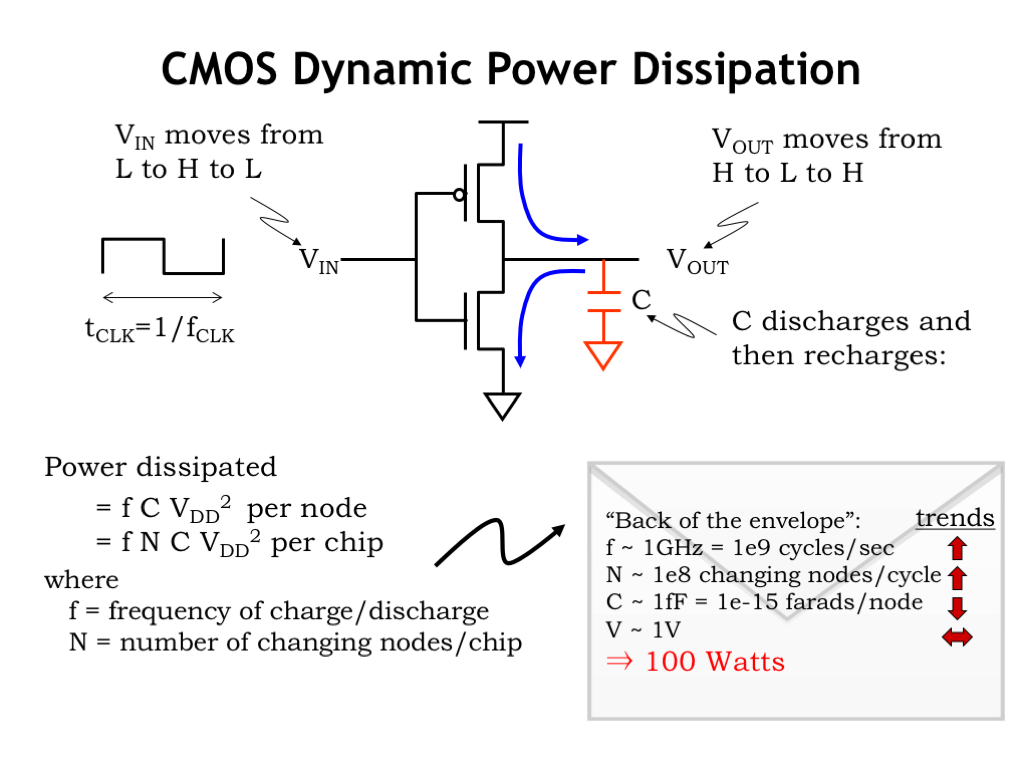
These results are summarized in the lower left. We’ve added the calculation for the energy dissipation of an entire circuit assuming N of the circuit’s nodes change each clock cycle.
How much energy could be consumed by a modern integrated circuit? Here’s a quick back-of-the-envelope estimate for a current generation CPU chip. It’s operating at, say, 1 GHz and will have 100 million internal nodes that could change each clock cycle. Each nodal capacitance is around 1 femtofarad and the power supply is about 1V. With these numbers, the estimated power consumption is 100 watts. We all know how hot a 100W light bulb gets! You can see it would be hard to keep the CPU from overheating.
This is way too much energy to be dissipated in many applications, and modern CPUs intended, say, for laptops only dissipate a fraction of this energy. So the CPU designers must have some tricks up their sleeve, some of which we’ll see in a minute.
But first notice how important it’s been to be able to reduce the power supply voltage in modern integrated circuits. If we’re able to reduce the power supply voltage from 3.3V to 1V, that alone accounts for more than a factor of 10 in power dissipation. So the newer circuit can be say, 5 times larger and 2 times faster with the same power budget!
Newer technologies trends are shown here. The net effect is that newer chips would naturally dissipate more power if we could afford to have them do so. We have to be very clever in how we use more and faster MOSFETs in order not to run up against the power dissipation constraints we face.
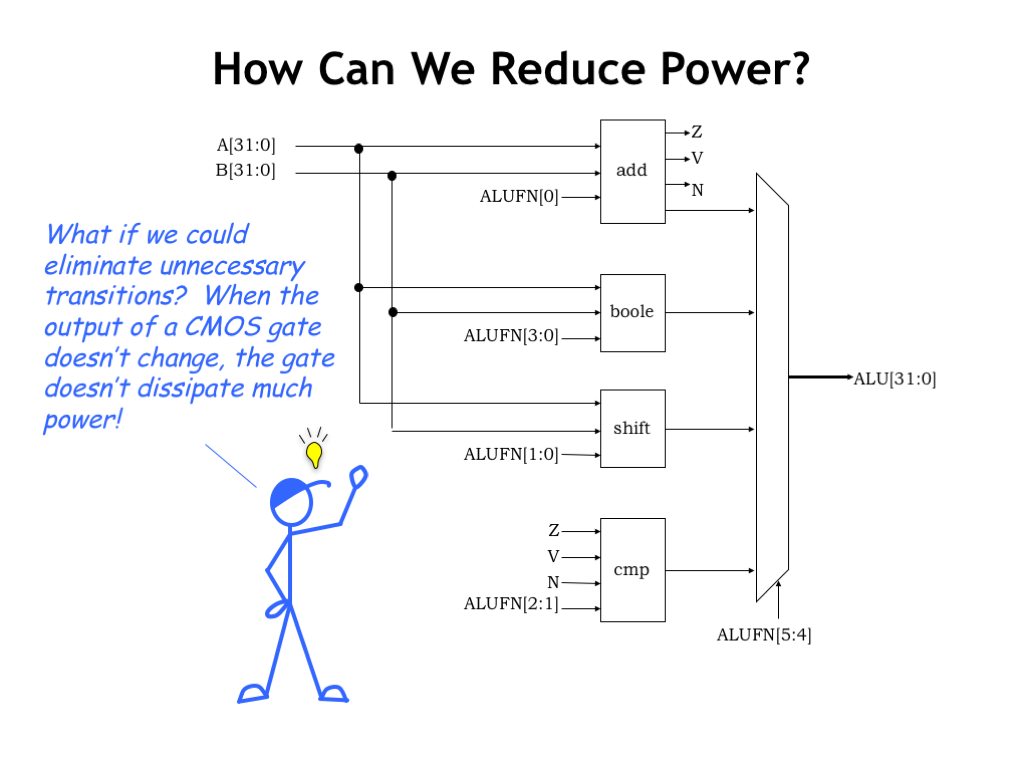
To see what we can do to reduce power consumption, consider the following diagram of an arithmetic and logic unit (ALU) like the one you’ll design in the final lab in this part of the course. There are four independent component modules, performing the separate arithmetic, Boolean, shifting and comparison operations typically found in an ALU. Some of the ALU control signals are used to select the desired result in a particular clock cycle, basically ignoring the answers produced by the other modules.
Of course, just because the other answers aren’t selected doesn’t mean we didn’t dissipate energy in computing them. This suggests an opportunity for saving power! Suppose we could somehow “turn off” modules whose outputs we didn’t need? One way to prevent them from dissipating power is to prevent the module’s inputs from changing, thus ensuring that no internal nodes would change and hence reducing the dynamic power dissipation of the “off” module to zero.
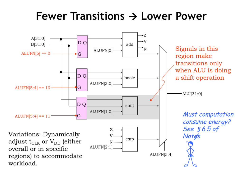
One idea is to put latches on the inputs to each module, only opening a module’s input latch if an answer was required from that module in the current cycle. If a module’s latch stayed closed, its internal nodes would remain unchanged, eliminating the module’s dynamic power dissipation. This could save a substantial amount of power. For example, the shifter circuitry has many internal nodes and so has a large dynamic power dissipation. But there are comparatively few shift operations in most programs, so with our proposed fix, most of the time those energy costs wouldn’t be incurred.
A more draconian approach to power conservation is to literally turn off unused portions of the circuit by switching off their power supply. This is more complicated to achieve, so this technique is usually reserved for special power-saving modes of operation, where we can afford the time it takes to reliably power the circuity back up.
Another idea is to slow the clock (reducing the frequency of nodal transitions) when there’s nothing for the circuit to do. This is particularly effective for devices that interact with the real world, where the time scales for significant external events are measured in milliseconds. The device can run slowly until an external event needs attention, then speed up the clock while it deals with the event.
All of these techniques and more are used in modern mobile devices to conserve battery power without limiting the ability to deliver bursts of performance. There is much more innovation waiting to be done in this area, something you may be asked to tackle as designers!
One last question is whether computation has to consume energy. There have been some interesting theoretical speculations about this question — see section 6.5 of the course notes to read more.
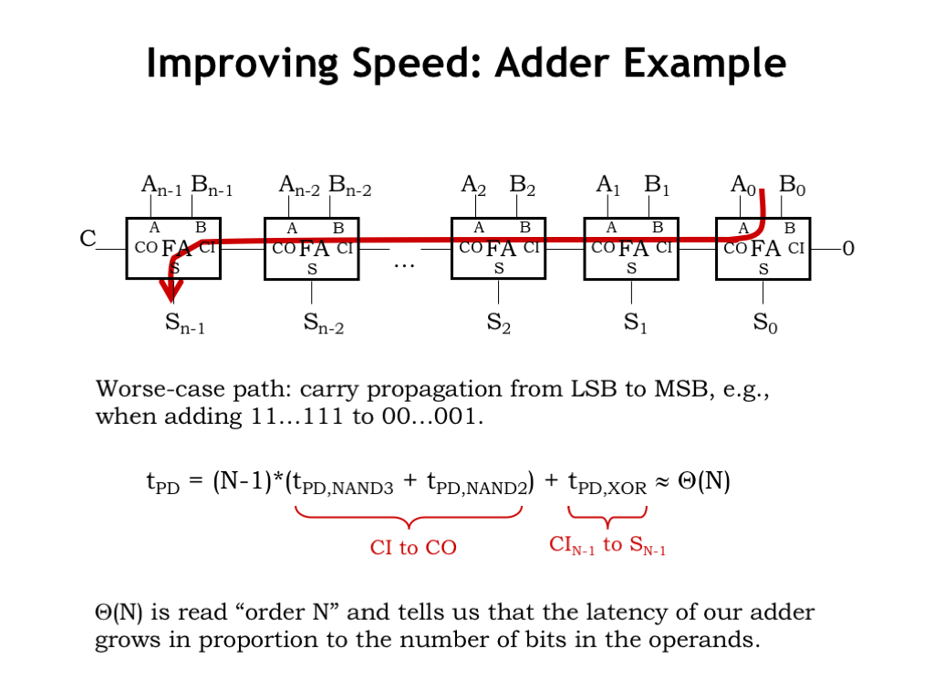
The most straightforward way to improve performance is to reduce the propagation delay of a circuit. Let’s look at a perennial performance bottleneck: the ripple-carry adder.
To fix it, we first have to figure out the path from inputs to outputs that has the largest propagation delay, i.e., the path that’s determining the overall \(t_{\textrm{PD}}\). In this case that path is the long carry chain following the carry-in to carry-out path through each full adder module. To trigger the path add -1 and 1 by setting the A inputs to all 1’s and the B input to all 0’s except for the low-order bit which is 1. The final answer is 0, but notice that each full adder has to wait for the carry-in from the previous stage before it produces 0 on its sum output and generates a carry-out for the next full adder. The carry really does ripple through the circuit as each full adder in turn does its thing.
To total propagation delay along this path is N-1 times the carry-in to carry-out delay of each full adder, plus the delay to produce the final bit of the sum.
How would the overall latency change if we, say, doubled the size of the operands, i.e., made N twice as large? It’s useful to summarize the dependency of the latency on N using the “order-of” notation to give us the big picture. Clearly as N gets larger the delay of the XOR gate at the end becomes less significant, so the order-of notation ignores terms that are relatively less important as N grows.
In this example, the latency is \(\Theta(N)\), which tells us that the latency would be expected to essentially double if we made N twice as large.
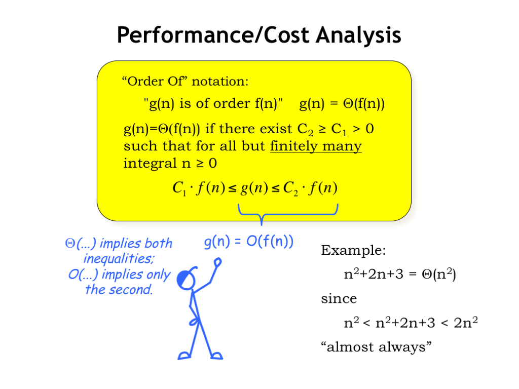
The order-of notation, which theoreticians call asymptotic analysis, tells us the term that would dominate the result as N grows. The yellow box contains the official definition, but an example might make it easier to understand what’s happening.
Suppose we want to characterize the growth in the value of the equation \(n^2 + 2n + 3\) as \(n\) gets larger. The dominant term is clearly \(n^2\) and the value of our equation is bounded above and below by simple multiples of \(n^2\), except for finitely many values of n. The lower bound is always true for \(n\) greater than or equal to 0. And in this case, the upper bound doesn’t hold only for \(n\) equal to 0, 1, 2, or 3. For all other positive values of \(n\) the upper inequality is true. So we’d say that this equation was \(\Theta(n^2)\).
There are actually two variants for the order-of notation. We use the \(\Theta()\) notation to indicate that \(g(n)\) is bounded above AND below by multiples of \(f(n)\). The \(O()\) notation is used when \(g(n)\) is only bounded above by a multiple of \(f(n)\).
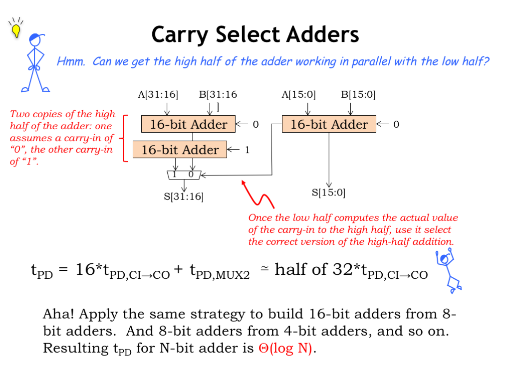
Here’s a first attempt at improving the latency of our addition circuit. The trouble with the ripple-carry adder is that the high-order bits have to wait for the carry-in from the low-order bits. Is there a way in which we can get high half the adder working in parallel with the low half?
Suppose we wanted to build a 32-bit adder. Let’s make two copies of the high 16 bits of the adder, one assuming the carry-in from the low 16 bits is 0, and the other assuming the carry-in is 1. So now we have three 16-bit adders, all of which can operate in parallel on newly arriving A and B inputs. Once the 16-bit additions are complete, we can use the actual carry-out from the low-half to select the answer from the particular high-half adder that used the matching carry-in value. This type of adder is appropriately named the carry-select adder.
The latency of this carry-select adder is just a little more than the latency of a 16-bit ripple-carry addition. This is approximately half the latency of the original 32-bit ripple-carry adder. So at a cost of about 50% more circuitry, we’ve halved the latency!
As a next step, we could apply the same strategy to halve the latency of the 16-bit adders. And then again to halve the latency of the 8-bit adders used in the previous step. At each step we halve the adder latency and add a MUX delay. After \(\log_2(N)\) steps, \(N\) will be 1 and we’re done.
At this point the latency would be some constant cost to do a 1-bit addition, plus \(\log_2(N)\) times the MUX latency to select the right answers. So the overall latency of the carry-select adder is \(\Theta(\log N)\). Note that \(\log_2 N\) and \(\log N\)only differ by a constant factor, so we ignore the base of the log in order-of notation.
The carry-select adder shows a clear performance-size tradeoff available to the designer.
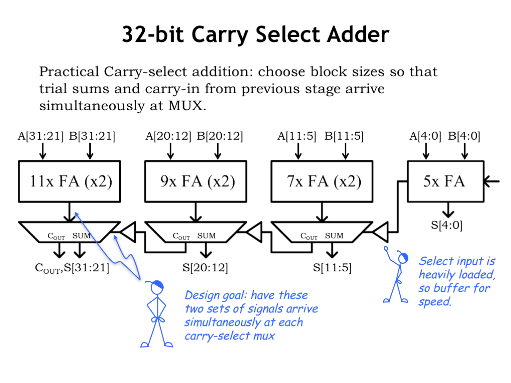
Since adders play a big role in many digital systems, here’s a more carefully engineered version of a 32-bit carry-select adder. You could try this in your ALU design!
The size of the adder blocks has been chosen so that the trial sums and the carry-in from the previous stage arrive at the carry-select MUX at approximately the same time. Note that since the select signal for the MUXes is heavily loaded we’ve included a buffer to make the select signal transitions faster.
This carry-select adder is about two-and-a-half times faster than a 32-bit ripple-carry adder at the cost of about twice as much circuitry. A great design to remember when you’re looking to double the speed of your ALU!
Here’s another approach to improving the latency of our adder, this time focusing just on the carry logic. Early on in the course, we learned that by going from a chain of logic gates to a tree of logic gates, we could go from a linear latency to a logarithmic latency. Let’s try to do that here.
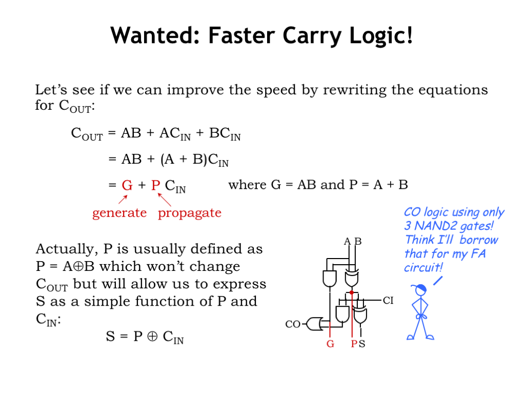
We’ll start by rewriting the equations for the carry-out from the full adder module. The final form of the rewritten equation has two terms. The G, or generate, term is true when the inputs will cause the module to generate a carry-out right away, without having to wait for the carry-in to arrive. The P, or propagate, term is true if the module will generate a carry-out only if there’s a carry-in.
So there only two ways to get a carry-out from the module: it’s either generated by the current module or the carry-in is propagated from the previous module.
Actually, it’s usual to change the logic for the P term from “A OR B” to “A XOR B”. This doesn’t change the truth table for the carry-out but will allow us to express the sum output as “P XOR carry-in”. Here’s the schematic for the reorganized full adder module. The little sum-of-products circuit for the carry-out can be implemented using 3 2-input NAND gates, which is a bit more compact than the implementation for the three product terms we suggested in Lab 2. Time to update your full adder circuit!
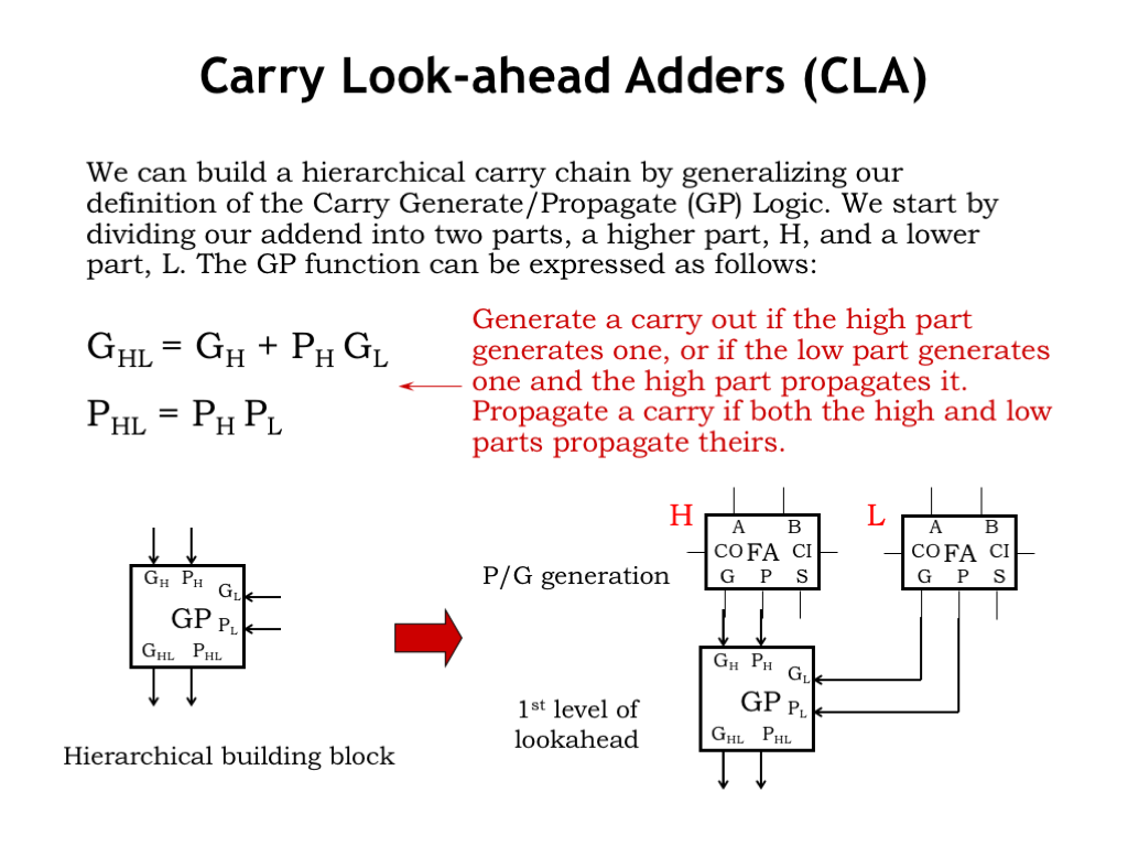
Now consider two adjacent adder modules in a larger adder circuit: we’ll use the label H to refer to the high-order module and the label L to refer to the low-order module.
We can use the generate and propagate information from each of the modules to develop equations for the carry-out from the pair of modules treated as a single block.
We’ll generate a carry-out from the block when a carry-out is generated by the H module, or when a carry-out is generated by the L module and propagated by the H module. And we’ll propagate the carry-in through the block only if the L module propagates its carry-in to the intermediate carry-out and H module propagates that to the final carry-out. So we have two simple equations requiring only a couple of logic gates to implement.
Let’s use these equations to build a generate-propagate (GP) module and hook it to the H and L modules as shown. The G and P outputs of the GP module tell us under what conditions we’ll get a carry-out from the two individual modules treated as a single, larger block.
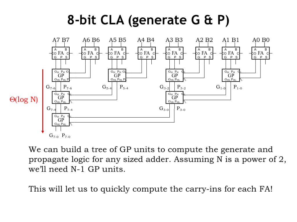
We can use additional layers of GP modules to build a tree of logic that computes the generate and propagate logic for adders with any number of inputs. For an adder with N inputs, the tree will contain a total of N-1 GP modules and have a latency that’s \(\Theta(\log N)\).
In the next step, we’ll see how to use the generate and propagate information to quickly compute the carry-in for each of the original full adder modules.
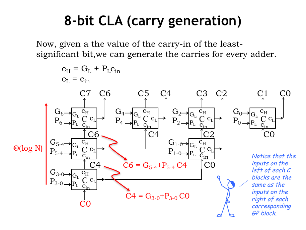
Once we’re given the carry-in \(C_0\) for the low-order bit, we can hierarchically compute the carry-in for each full adder module.
Given the carry-in to a block of adders, we simply pass it along as the carry-in to the low-half of the block. The carry-in for the high-half of the block is computed the using the generate and propagate information from the low-half of the block.
We can use these equations to build a C module and arrange the C modules in a tree as shown to use the \(C_0\) carry-in to hierarchically compute the carry-in to each layer of successively smaller blocks, until we finally reach the full adder modules. For example, these equations show how \(C_4\) is computed from \(C_0\), and \(C_6\) is computed from \(C_4\).
Again the total propagation delay from the arrival of the \(C_0\) input to the carry-ins for each full adder is \(\Theta(\log N)\).
Notice that the \(G_L\) and \(P_L\) inputs to a particular C module are the same as two of the inputs to the GP module in the same position in the GP tree.
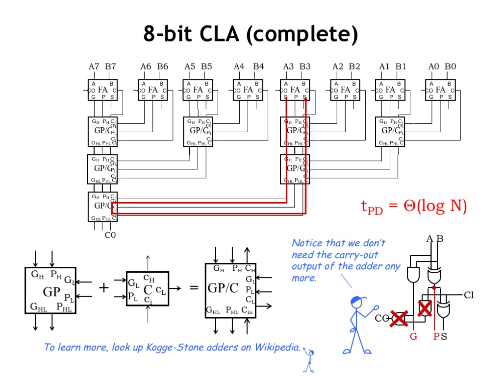
We can combine the GP module and C module to form a single carry-lookahead module that passes generate and propagate information up the tree and carry-in information down the tree. The schematic at the top shows how to wire up the tree of carry-lookahead modules.
And now we get to the payoff for all this hard work! The combined propagation delay to hierarchically compute the generate and propagate information on the way up and the carry-in information on the way down is \(\Theta(\log N)\), which is then the latency for the entire adder since computing the sum outputs only takes one additional XOR delay. This is a considerable improvement over the \(\Theta(N)\) latency of the ripple-carry adder.
A final design note: we no longer need the carry-out circuitry in the full adder module, so it can be removed.
Variations on this generate-propagate strategy form the basis for the fastest-known adder circuits. If you’d like to learn more, look up “Kogge-Stone adders” on Wikipedia.
One of the biggest and slowest circuits in an arithmetic and logic unit is the multiplier. We’ll start by developing a straightforward implementation and then, in the next section, look into tradeoffs to make it either smaller or faster.
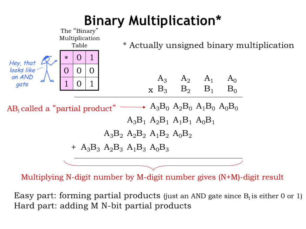
Here’s the multiplication operation for two unsigned 4-bit operands broken down into its component operations. This is exactly how we learned to do it in primary school. We take each digit of the multiplier (the B operand) and use our memorized multiplication tables to multiply it with each digit of the multiplicand (the A operand), dealing with any carries into the next column as we process the multiplicand right-to-left. The output from this step is called a partial product, and then we repeat the step for the remaining bits of the multiplier. Each partial product is shifted one digit to the left, reflecting the increasing weight of the multiplier digits.
In our case the digits are just single bits, i.e., they’re 0 or 1 and the multiplication table is pretty simple! In fact, the 1-bit-by-1-bit binary multiplication circuit is just a 2-input AND gate. And look Mom, no carries!
The partial products are N bits wide since there are no carries. If the multiplier has M bits, there will be M partial products. And when we add the partial products together, we’ll get an N+M bit result if we account for the possible carry-out from the high-order bit.
The easy part of the multiplication is forming the partial products — it just requires some AND gates. The more expensive operation is adding together the M N-bit partial products.
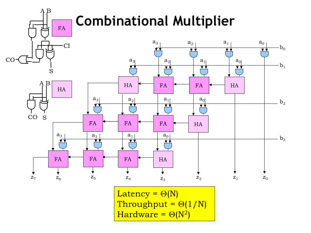
Here’s the schematic for the combinational logic needed to implement the 4x4 multiplication, which would be easy to extend for larger multipliers (we’d need more rows) or larger multiplicands (we’d need more columns).
The M*N 2-input AND gates compute the bits of the M partial products. The adder modules add the current row’s partial product with the sum of the partial products from the earlier rows. Actually there are two types of adder modules. The full adder is used when the modules needs three inputs. The simpler half adder is used when only two inputs are needed.
The longest path through this circuit takes a moment to figure out. Information is always moving either down a row or left to the adjacent column. Since there are M rows and, in any particular row, N columns, there are at most N+M modules along any path from input to output. So the latency is \(\Theta(N)\), since M and N differ by just some constant factor.
Since this is a combinational circuit, the throughput is just 1/latency. And the total amount of hardware is \(\Theta(N^2)\).
In the next section, we’ll investigate how to reduce the hardware costs, or, separately, how to increase the throughput.
But before we do that, let’s take a moment to see how the circuit would change if the operands were two’s complement integers instead of unsigned integers.
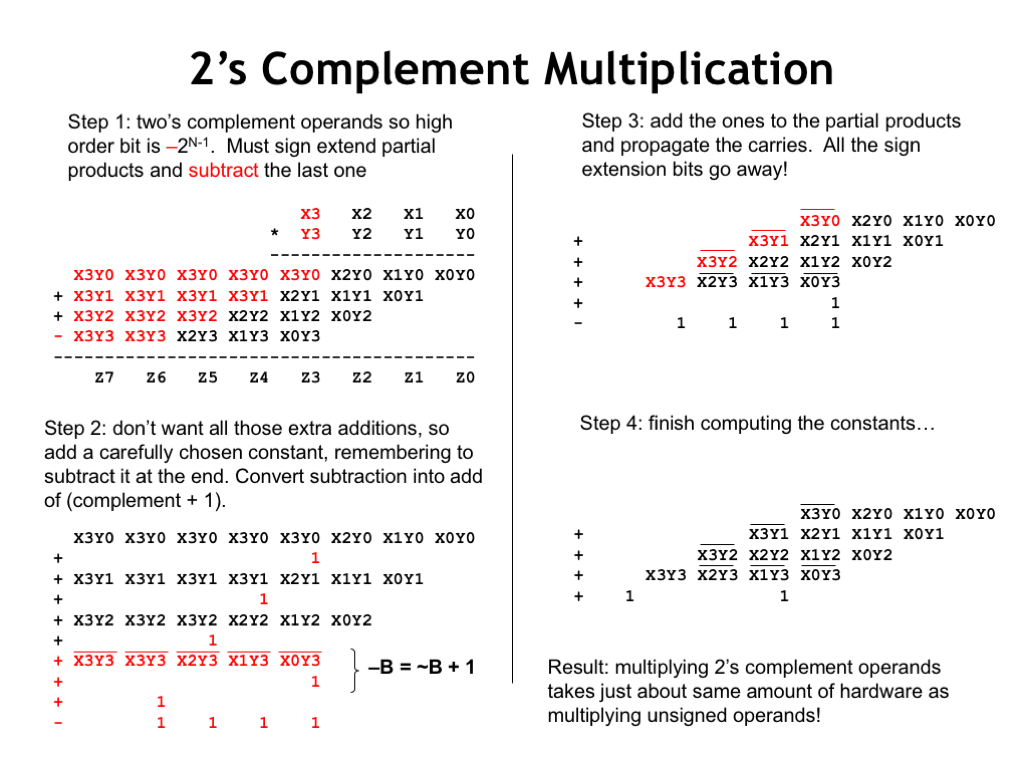
With a two’s complement multiplier and multiplicand, the high-order bit of each has negative weight. So when adding together the partial products, we’ll need to sign-extend each of the N-bit partial products to the full N+M-bit width of the addition. This will ensure that a negative partial product is properly treated when doing the addition. And, of course, since the high-order bit of the multiplier has a negative weight, we’d subtract instead of add the last partial product.
Now for the clever bit. We’ll add 1’s to various of the columns and then subtract them later, with the goal of eliminating all the extra additions caused by the sign-extension. We’ll also rewrite the subtraction of the last partial product as first complementing the partial product and then adding 1. This is all a bit mysterious but…
Here in step 3 we see the effect of all the step 2 machinations. Let’s look at the high order bit of the first partial product X3Y0. If that partial product is non-negative, X3Y0 is a 0, so all the sign-extension bits are 0 and can be removed. The effect of adding a 1 in that position is to simply complement X3Y0.
On the other hand, if that partial product is negative, X3Y0 is 1, and all the sign-extension bits are 1. Now when we add a 1 in that position, we complement the X3Y0 bit back to 0, but we also get a carry-out. When that’s added to the first sign-extension bit (which is itself a 1), we get zero with another carry-out. And so on, with all the sign-extension bits eventually getting flipped to 0 as the carry ripples to the end. Again the net effect of adding a 1 in that position is to simply complement X3Y0.
We do the same for all the other sign-extended partial products, leaving us with the results shown here.
In the final step we do a bit of arithmetic on the remaining constants to end up with this table of work to be done. Somewhat to our surprise, this isn’t much different than the original table for the unsigned multiplication. There are a few partial product bits that need to be complemented, and two 1-bits that need to be added to particular columns.
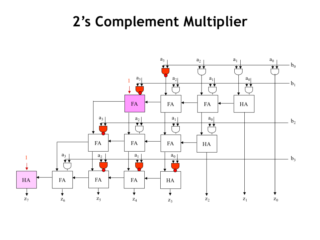
The resulting circuitry is shown here. We’ve changed some of the AND gates to NAND gates to perform the necessary complements. And we’ve changed the logic necessary to deal with the two 1-bits that needed to be added in.
The colored elements show the changes made from the original unsigned multiplier circuitry. Basically, the circuit for multiplying two’s complement operands has the same latency, throughput and hardware costs as the original circuitry.
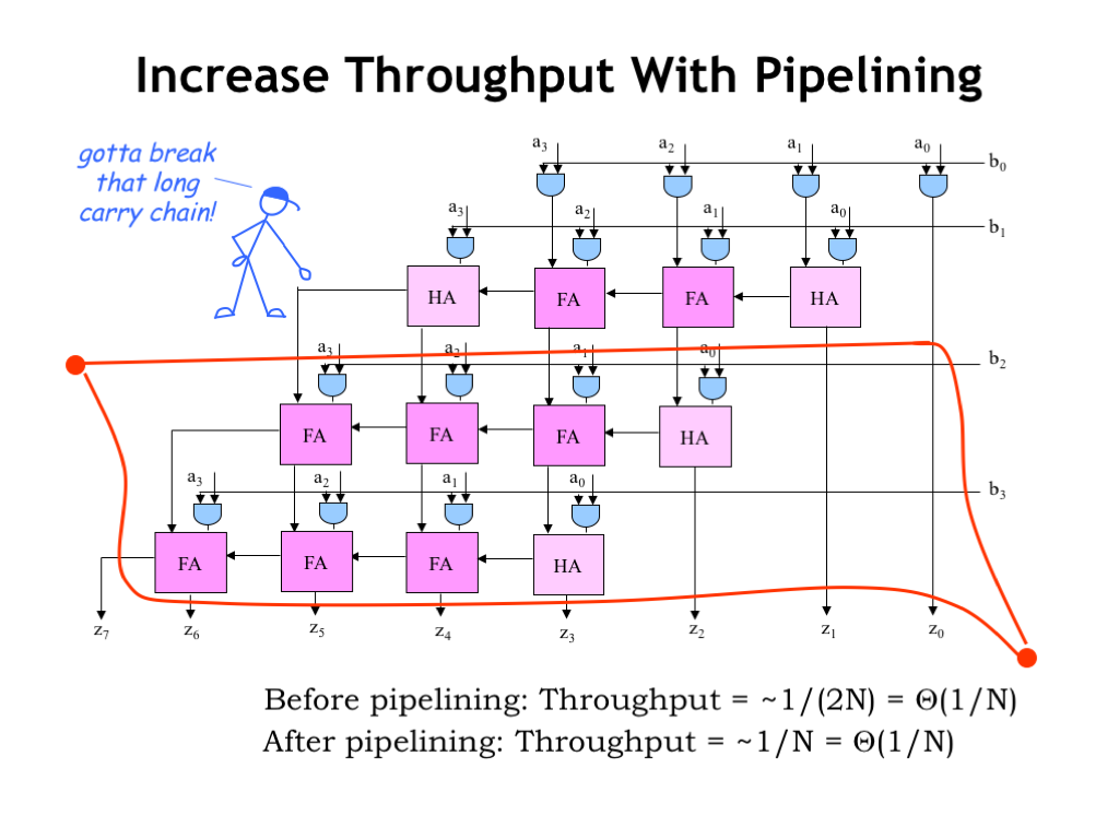
Let’s see if we can improve the throughput of the original combinational multiplier design. We’ll use our patented pipelining process to divide the processing into stages with the expectation of achieving a smaller clock period and higher throughput. The number to beat is approximately 1 output every 2N, where N is the number of bits in each of the operands.
Our first step is to draw a contour across all the outputs. This creates a 1-pipeline, which gets us started but doesn’t improve the throughput.
Let’s add another contour, dividing the computations about in half. If we’re on the right track, we hope to see some improvement in the throughput. And indeed we do: the throughput has doubled. Yet both the before and after throughputs are \(\Theta(1/N)\). Is there any hope of a dramatically better throughput?
The necessary insight is that as long as an entire row is inside a single pipeline stage, the latency of the stage will be \(\Theta(N)\) since we have to leave time for the N-bit ripple-carry add to complete.
There are several ways to tackle this problem. The technique illustrated here will be useful in our next task. In this schematic we’ve redrawn the carry chains. Carry-outs are still connected to a module one column to the left, but, in this case, a module that’s down a row. So all the additions that need to happen in a specific column still happen in that column, we’ve just reorganized which row does the adding.
Let’s pipeline this revised diagram, creating stages with approximately two modules’ worth of propagation delay.
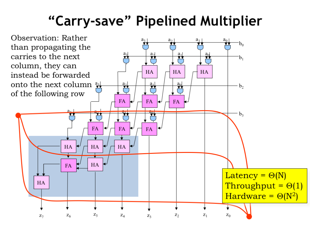
The horizontal contours now break the long carry chains and the latency of each stage is now constant, independent of N.
Note that we had to add \(\Theta(N)\) extra rows to take care of propagating the carries all the way to the end — the extra circuitry is shown in the grey box.
To achieve a latency that’s independent of N in each stage, we’ll need \(\Theta(N)\) contours. This means the latency is constant, which in order-of notation we write as \(\Theta(1)\). But this means the clock period is now independent of N, as is the throughput — they are both \(\Theta(1)\). With \(\Theta(N)\) contours, there are \(\Theta(N)\) pipeline stages, so the system latency is \(\Theta(N)\). The hardware cost is still \(\Theta(N^2)\). So the pipelined carry-save multiplier has dramatically better throughput than the original circuit, another design tradeoff we can remember for future use.
We’ll use the carry-save technique in our next optimization, which is to implement the multiplier using only \(\Theta(N)\) hardware.
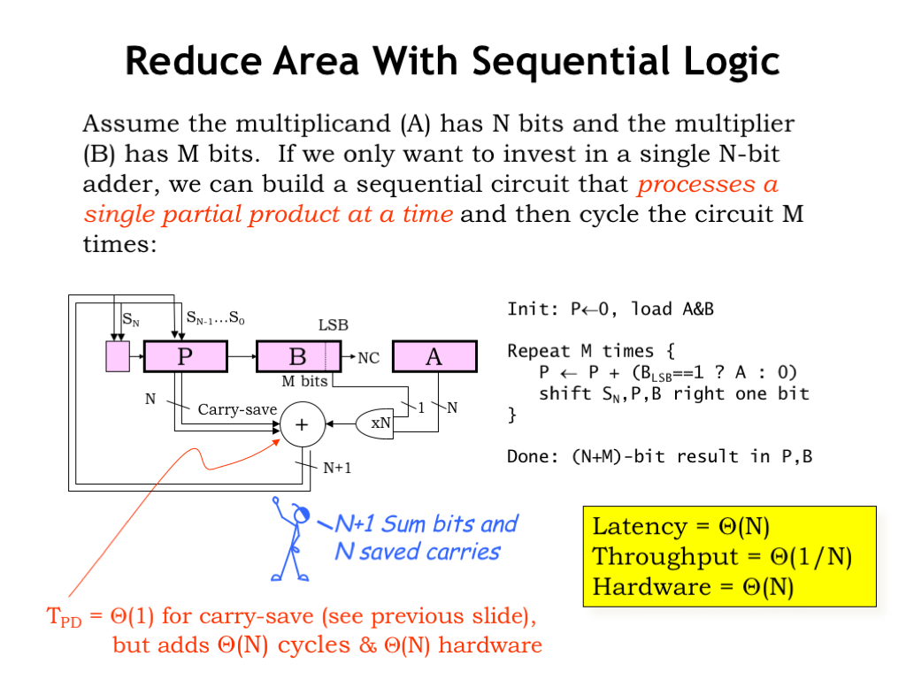
This sequential multiplier design computes a single partial product in each step and adds it to the accumulating sum. It will take \(\Theta(N)\) steps to perform the complete multiplication.
In each step, the next bit of the multiplier, found in the low-order bit of the B register, is ANDed with the multiplicand to form the next partial product. This is sent to the N-bit carry-save adder to be added to the accumulating sum in the P register. The value in the P register and the output of the adder are in “carry-save format”. This means there are 32 data bits, but, in addition, 31 saved carries, to be added to the appropriate column in the next cycle. The output of the carry-save adder is saved in the P register, then in preparation for the next step both P and B are shifted right by 1 bit. So each cycle one bit of the accumulated sum is retired to the B register since it can no longer be affected by the remaining partial products. Think of it this way: instead of shifting the partial products left to account for the weight of the current multiplier bit, we’re shifting the accumulated sum right!
The clock period needed for the sequential logic is quite small, and, more importantly is independent of N. Since there’s no carry propagation, the latency of the carry-save adder is very small, i.e., only enough time for the operation of a single full adder module.
After \(\Theta(N)\) steps, we’ve generated the necessary partial products, but will need to continue for another \(\Theta(N)\) steps to finish propagating the carries through the carry-save adder.
But even at 2N steps, the overall latency of the multiplier is still \(\Theta(N)\). And at the end of the 2N steps, we produce the answer in the P and B registers combined, so the throughput is \(\Theta(1/N)\). The big change is in the hardware cost at \(\Theta(N)\), a dramatic improvement over the \(\Theta(N^2)\) hardware cost of the original combinational multiplier.
This completes our little foray into multiplier designs. We’ve seen that with a little cleverness we can create designs with \(\Theta(1)\) throughput, or designs with only \(\Theta(N)\) hardware. The technique of carry-save addition is useful in many situations and its use can improve throughput at constant hardware cost, or save hardware at a constant throughput.
This discussion of design tradeoffs completes Part 1 of the course. We’ve covered a lot of ground in the last eight lectures.
We started by looking at the mathematics underlying information theory and used it to help evaluate various alternative ways of effectively using sequences of bits to encode information content. Then we turned our attention to adding carefully-chosen redundancies to our encoding to ensure that we could detect and even correct errors that corrupted our bit-level encodings.
Next we learned how analog signaling accumulates errors as we added processing elements to our system. We solved the problem by using voltages “digitally” choosing two ranges of voltages to encode the bit values 0 and 1. We had different signaling specifications for outputs and inputs, adding noise margins to make our signaling more robust. Then we developed the static discipline for combinational devices and were led to the conclusion that our devices had to be non-linear and exhibit gains > 1.
In our study of combinational logic, we fist learned about the MOSFET, a voltage-controlled switch. We developed a technique for using MOSFETs to build CMOS combinational logic gates, which met all the criteria of the static discipline. Then we discussed systematic ways of synthesizing larger combinational circuits that could implement any functionality we could express in the form of a truth table.
To be able to perform sequences of operations, we first developed a reliable bistable storage element based on a positive feedback loop. To ensure the storage elements worked correctly we imposed the dynamic discipline which required inputs to the storage elements to be stable just before and after the time the storage element was transitioned to “memory mode”. We introduced finite-state machines as a useful abstraction for designing sequential logic. And then we figured out how to deal with asynchronous inputs in way that minimized the chance of incorrect operation due to metastability.
In the last two lectures we developed latency and throughput as performance measures for digital systems and discussed ways of achieving maximum throughput under various constraints. We discussed how it’s possible to make tradeoffs to achieve goals of minimizing power dissipation and increasing performance through decreased latency or increased throughput.
Whew! That’s a lot of information in a short amount of time.


