
.toc { margin-left: 2em; } .lecslide { margin-top: 1em; margin-bottom: 1em; border-top: 0.5px solid #808080; padding-top: 1em; text-align: center; } .lecslideimg { width: 5in; border: 1px solid black; }
- Example: Factorial I
- Example: Factorial II
- Datapath for Factorial
- Control FSM for Factorial
- Control FSM Hardware
- So Far: Single-Purpose Hardware
- A Simple Programmable Datapath
- A Control FSM for Factorial
- New Problem → New Control FSM
- The ENIAC Computer
- Programming The ENIAC
- The von Neumann Model
- Key Idea: Stored-Program Computer
- Anatomy of a von Neumann Computer
- Instructions
- Instruction Set Architecture (ISA)
- ISA Design
- Beta ISA: Storage
- Storage Conventions
- Beta ISA: Instructions
- Beta ALU Instructions
- Implementation Sketch #1
- Should We Support Constant Operands?
- Beta ALU Instructions with Constant
- Implementation Sketch #2
- Beta Load and Store Instructions
- Using LD and ST
- Can We Solve Factorial with ALU Instructions?
- Beta Branch Instructions
- Can We Solve Factorial Now?
- Beta JMP Instruction
- Beta ISA Summary
Content of the following slides is described in the surrounding text.
Welcome to Part 2 of 6.004! In this part of the course, we turn our attention to the design and implementation of digital systems that can perform useful computations on different types of binary data. We’ll come up with a general-purpose design for these systems, we which we call “computers”, so that they can serve as useful tools in many diverse application areas. Computers were first used to perform numeric calculations in science and engineering, but today they are used as the central control element in any system where complex behavior is required.
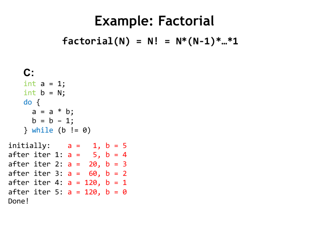
We have a lot to do in this lecture, so let’s get started! Suppose we want to design a system to compute the factorial function on some numeric argument N. N! is defined as the product of N times N-1 times N-2, and so on down to 1.
We can use a programming language like C to describe the sequence of operations necessary to perform the factorial computation. In this program there are two variables, “a” and “b”. “a” is used to accumulate the answer as we compute it step-by-step. “b” is used to hold the next value we need to multiply. “b” starts with the value of the numeric argument N. The DO loop is where the work gets done: on each loop iteration we perform one of the multiplies from the factorial formula, updating the value of the accumulator “a” with the result, then decrementing “b” in preparation for the next loop iteration.
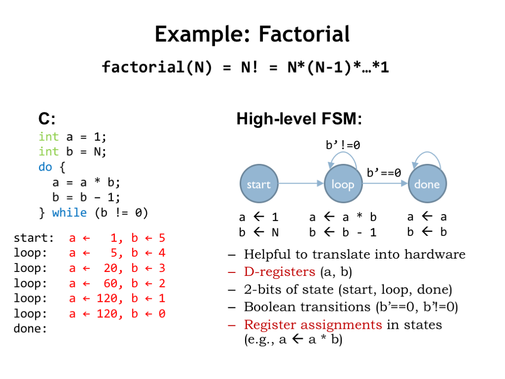
If we want to implement a digital system that performs this sequence of operations, it makes sense to use sequential logic! Here’s the state transition diagram for a high-level finite-state machine designed to perform the necessary computations in the desired order. We call this a high-level FSM since the “outputs” of each state are more than simple logic levels. They are formulas indicating operations to be performed on source variables, storing the result in a destination variable.
The sequence of states visited while the FSM is running mirrors the steps performed by the execution of the C program. The FSM repeats the LOOP state until the new value to be stored in “b” is equal to 0, at which point the FSM transitions into the final DONE state.
The high-level FSM is useful when designing the circuitry necessary to implement the desired computation using our digital logic building blocks. We’ll use 32-bit D-registers to hold the “a” and “b” values. And we’ll need a 2-bit D-register to hold the 2-bit encoding of the current state, i.e., the encoding for either START, LOOP or DONE. We’ll include logic to compute the inputs required to implement the correct state transitions. In this case, we need to know if the new value for “b” is zero or not. And, finally, we’ll need logic to perform multiply and decrement, and to select which value should be loaded into the “a” and “b” registers at the end of each FSM cycle.
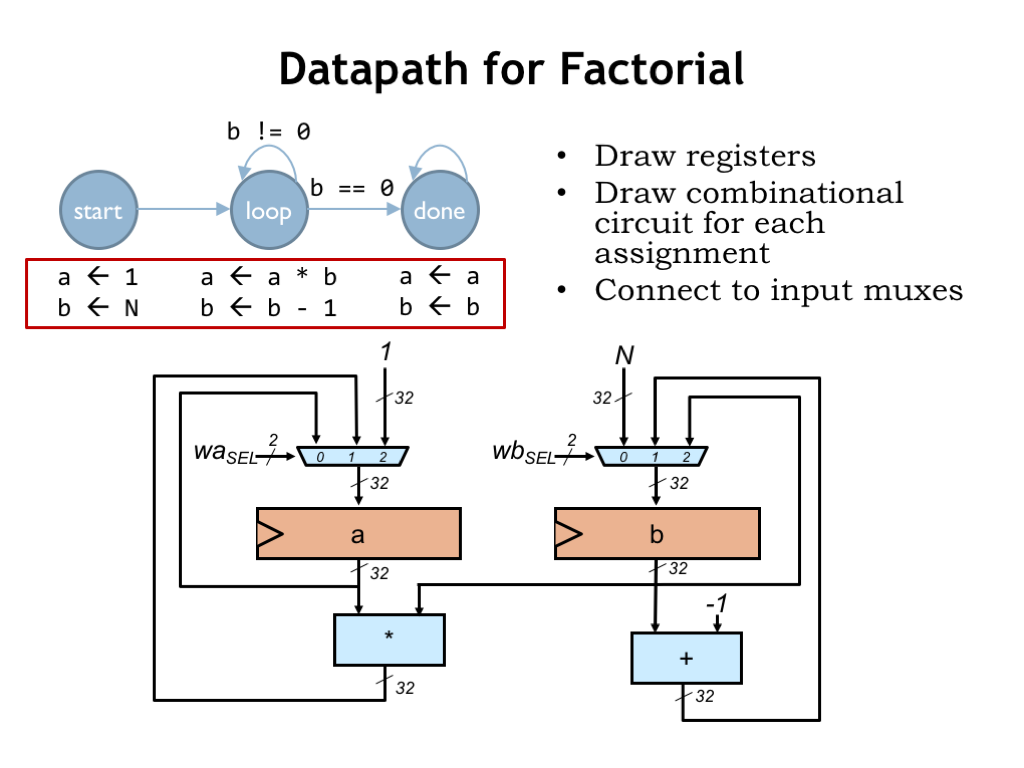
Let’s start by designing the logic that implements the desired computations — we call this part of the logic the “datapath”.
First we’ll need two 32-bit D-registers to hold the “a” and “b” values. Then we’ll draw the combinational logic blocks needed to compute the values to be stored in those registers. In the START state, we need the constant 1 to load into the “a” register and the constant N to load into the “b” register. In the LOOP state, we need to compute a*b for the “a” register and b-1 for the “b” register. Finally, in the DONE state, we need to be able to reload each register with its current value.
We’ll use multiplexers to select the appropriate value to load into each of the data registers. These multiplexers are controlled by 2-bit select signals that choose which of the three 32-bit input values will be the 32-bit value to be loaded into the register. So by choosing the appropriate values for WASEL and WBSEL, we can make the datapath compute the desired values at each step in the FSM’s operation.
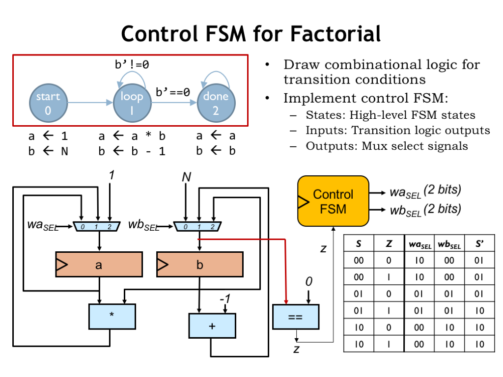
Next we’ll add the combinational logic needed to control the FSM’s state transitions. In this case, we need to test if the new value to be loaded into the “b” register is zero. The Z signal from the datapath will be 1 if that’s the case and 0 otherwise.
Now we’re all set to add the hardware for the control FSM, which has one input (Z) from the datapath and generates two 2-bit outputs (WASEL and WBSEL) to control the datapath. Here’s the truth table for the FSM’s combinational logic. S is the current state, encoded as a 2-bit value, and S’ is the next state.
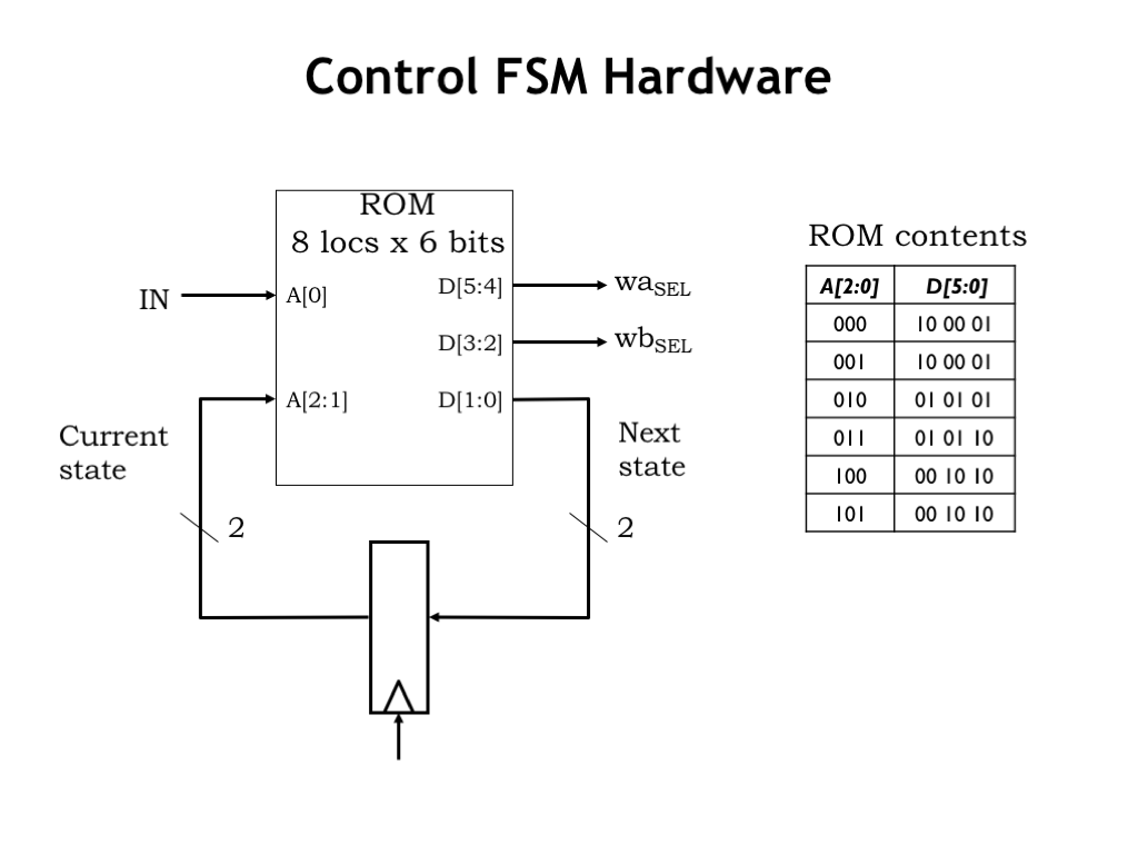
Using our skills from Part 1 of the course, we’re ready to draw a schematic for the system! We know how to design the appropriate multiplier and decrement circuitry. And we can use our standard register-and-ROM implementation for the control FSM. The Z signal from the datapath is combined with the 2 bits of current state to form the 3 inputs to the combinational logic, in this case realized by a read-only memory with \(2^3=8\) locations. Each ROM location has the appropriate values for the 6 output bits: 2 bits each for WASEL, WBSEL, and next state. The table on the right shows the ROM contents, which are easily determined from the table on the previous slide.
Okay, we’ve figured out a way to design hardware to perform a particular computation: Draw the state transition diagram for an FSM that describes the sequence of operations needed to complete the computation. Then construct the appropriate datapath, using registers to store values and combinational logic to implement the needed operations. Finally build an FSM to generate the control signals required by the datapath.
Is the datapath plus control logic itself an FSM? Well, it has registers and some combinational logic, so, yes, it is an FSM. Can we draw the truth table? In theory, yes. In practice, there are 66 bits of registers and hence 66 bits of state, so our truth table would need \(2^{66}\) rows! Hmm, not very likely that we’d be able to draw the truth table! The difficulty comes from thinking of the registers in the datapath as part of the state of our super-FSM. That’s why we think about the datapath as being separate from the control FSM.
So how do we generalize this approach so we can use one computer circuit to solve many different problems? Well, most problems would probably require more storage for operands and results. And a larger list of allowable operations would be handy. This is actually a bit tricky: what’s the minimum set of operations we can get away with? As we’ll see later, surprisingly simple hardware is sufficient to perform any realizable computation. At the other extreme, many complex operations (e.g., fast fourier transform) are best implemented as sequences of simpler operations (e.g., add and multiply) rather than as a single massive combinational circuit. These sorts of design tradeoffs are what makes computer architecture fun!
We’d then combine our larger storage with logic for our chosen set of operations into a general purpose datapath that could be reused to solve many different problems. Let’s see how that would work…
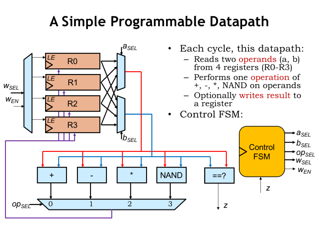
Here’s a datapath with 4 data registers to hold results. The ASEL and BSEL multiplexers allow any of the data registers to be selected as either operand for our repertoire of arithmetic and boolean operations. The result is selected by the OPSEL MUX and can be written back into any of the data registers by setting the WEN control signal to 1 and using the 2-bit WSEL signal to select which data register will be loaded at the next rising clock edge. Note that the data registers have a load-enable control input: when this signal is 1, the register will load a new value from its D input, otherwise it ignores the D input and simply reloads its previous value.
And, of course, we’ll add a control FSM to generate the appropriate sequence of control signals for the datapath. The Z input from the datapath allows the system to perform data-dependent operations, where the sequence of operations can be influenced by the actual values in the data registers.
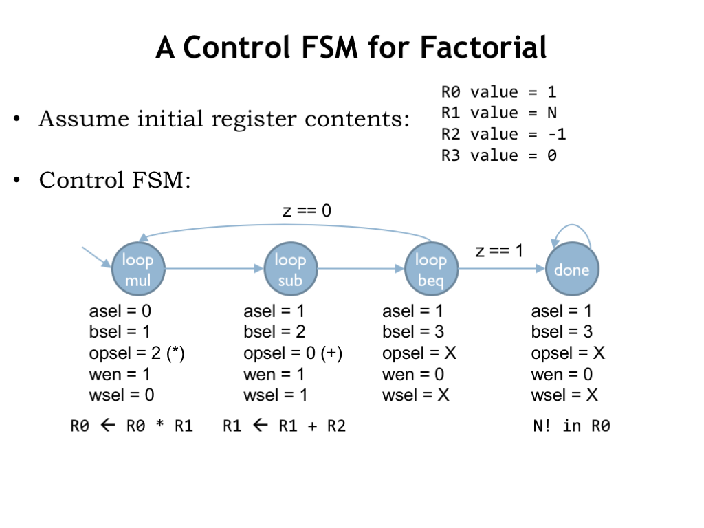
Here’s the state transition diagram for the control FSM we’d use if we wanted to use this datapath to compute factorial assuming the initial contents of the data registers are as shown. We need a few more states than in our initial implementation since this datapath can only perform one operation at each step. So we need three steps for each iteration: one for the multiply, one for the decrement, and one for the test to see if we’re done.
As seen here, it’s often the case that general-purpose computer hardware will need more cycles and perhaps involve more hardware than an optimized single-purpose circuit.
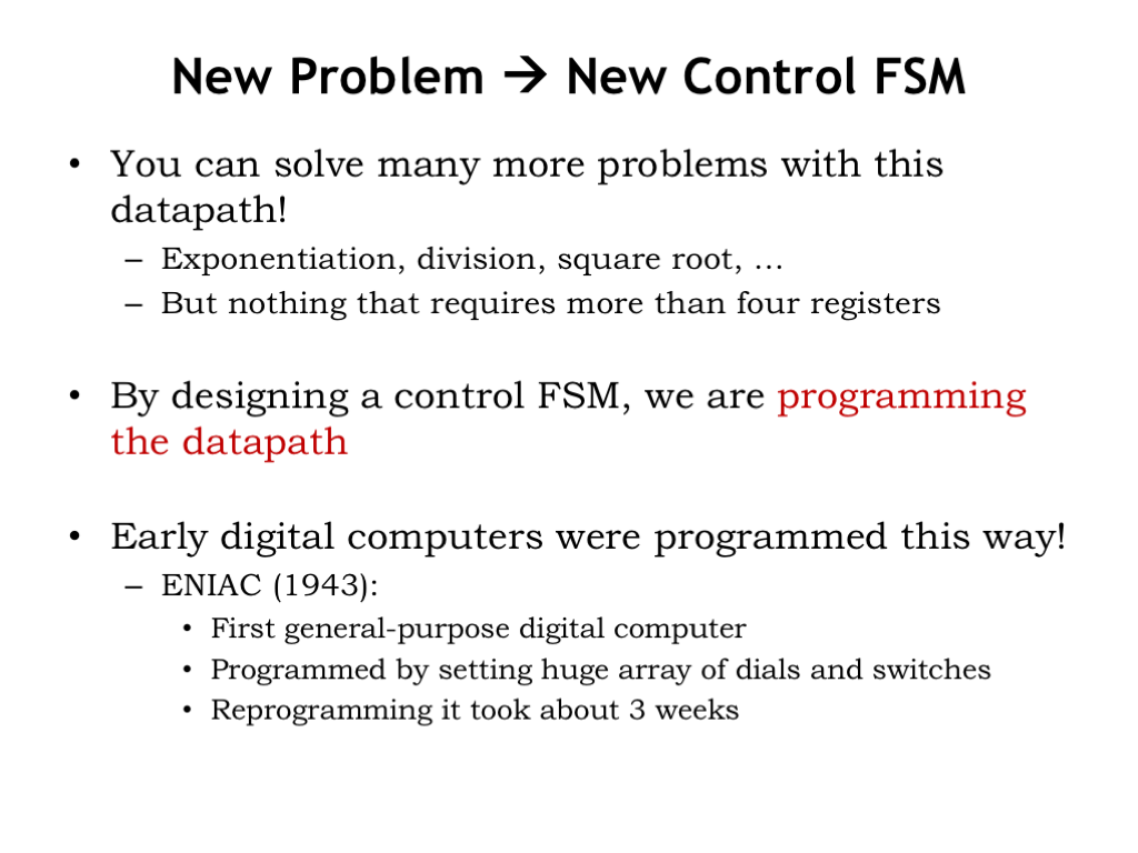
You can solve many different problems with this system: exponentiation, division, square root, and so on, so long as you don’t need more than four data registers to hold input data, intermediate results, or the final answer.
By designing a control FSM, we are in effect “programming” our digital system, specifying the sequence of operations it will perform.
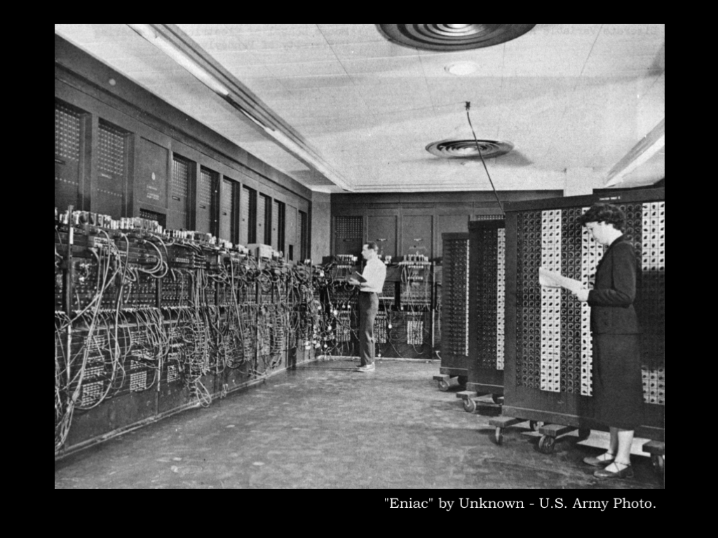
This is exactly how the early digital computers worked! Here’s a picture of the ENIAC computer built in 1943 at the University of Pennsylvania.
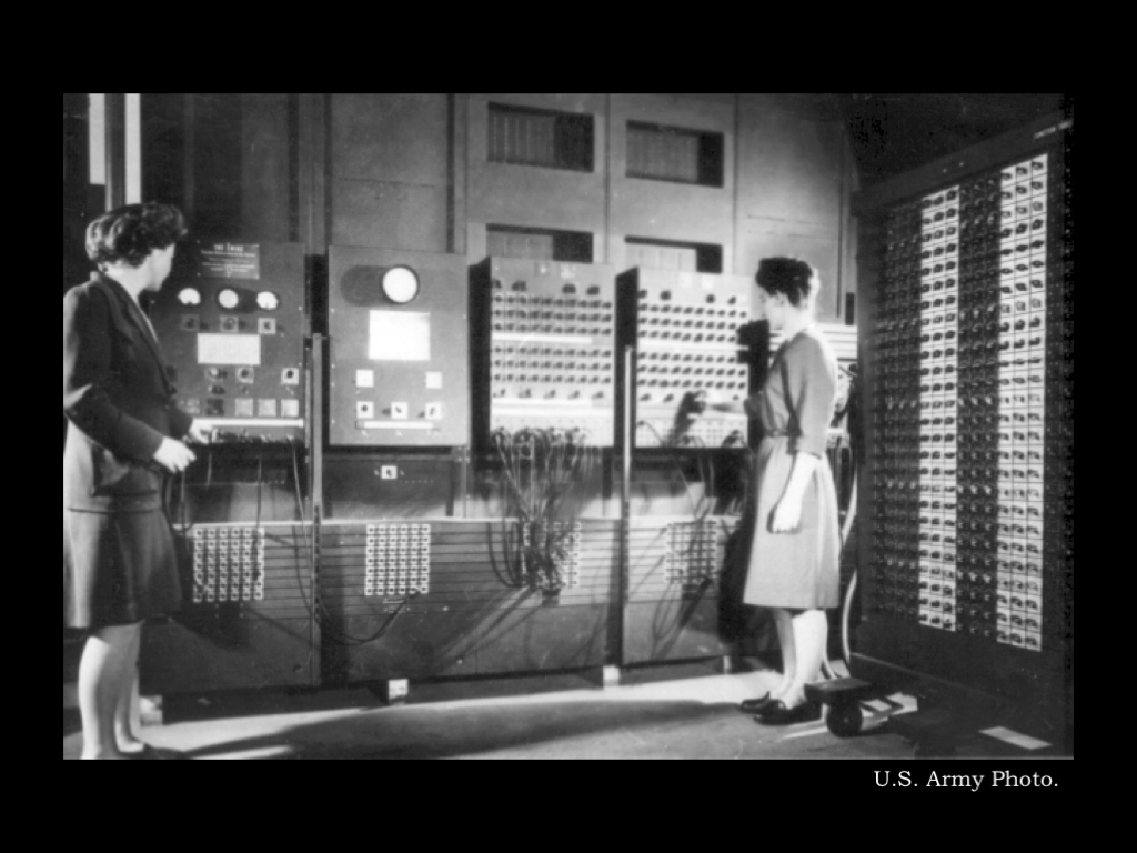
The Wikipedia article on the ENIAC tells us that “ENIAC could be programmed to perform complex sequences of operations, including loops, branches, and subroutines. The task of taking a problem and mapping it onto the machine was complex, and usually took weeks. After the program was figured out on paper, the process of getting the program into ENIAC by manipulating its switches and cables could take days. This was followed by a period of verification and debugging, aided by the ability to execute the program step by step.”
It’s clear that we need a less cumbersome way to program our computer!
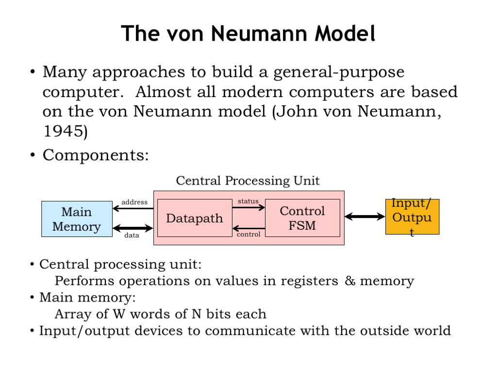
There are many approaches to building a general-purpose computer that can be easily re-programmed for new problems. Almost all modern computers are based on the “stored program” computer architecture developed by John von Neumann in 1945, which is now commonly referred to as the “von Neumann model”.
The von Neumann model has three components. There’s a central processing unit (aka the CPU) that contains a datapath and control FSM as described previously.
The CPU is connected to a read/write memory that holds some number W of words, each with N bits. Nowadays, even small memories have a billion words and the width of each location is at least 32 bits (usually more). This memory is often referred to as “main memory” to distinguish it from other memories in the system. You can think of it as an array: when the CPU wishes to operate on values in memory, it sends the memory an array index, which we call the address, and, after a short delay (currently 10’s of nanoseconds) the memory will return the N-bit value stored at that address. Writes to main memory follow the same protocol except, of course, the data flows in the opposite direction. We’ll talk about memory technologies a couple of lectures from now.
And, finally, there are input/output devices that enable the computer system to communicate with the outside world or to access data storage that, unlike main memory, will remember values even when turned off.
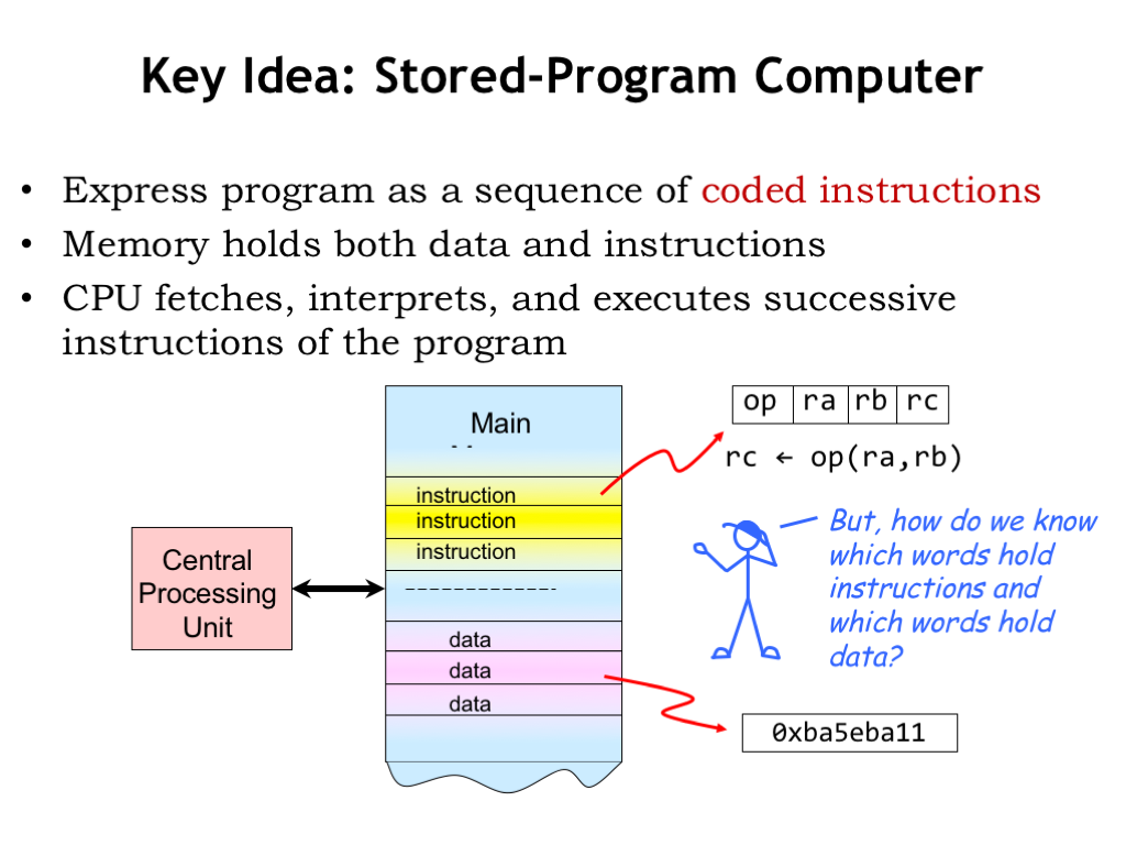
The key idea is to use main memory to hold the instructions for the CPU as well as data. Both instructions and data are, of course, just binary data stored in main memory.
Interpreted as an instruction, a value in memory can be thought of as a set of fields containing one or more bits encoding information about the actions to be performed by the CPU. The opcode field indicates the operation to be performed (e.g., ADD, XOR, COMPARE). Subsequent fields specify which registers supply the source operands and the destination register where the result is stored. The CPU interprets the information in the instruction fields and performs the requested operation. It would then move on to the next instruction in memory, executing the stored program step-by-step. The goal of this chapter is to discuss the details of what operations we want the CPU to perform, how many registers we should have, and so on.
Of course, some values in memory are not instructions! They might be binary data representing numeric values, strings of characters, and so on. The CPU will read these values into its temporary registers when it needs to operate on them and write newly computed values back into memory.
Mr. Blue is asking a good question: how do we know which words in memory are instructions and which are data? After all, they’re both binary values! The answer is that we can’t tell by looking at the values — it’s how they are used by the CPU that distinguishes instructions from data. If a value is loaded into the datapath, it’s being used as data. If a value is loaded by the control logic, it’s being used as an instruction.
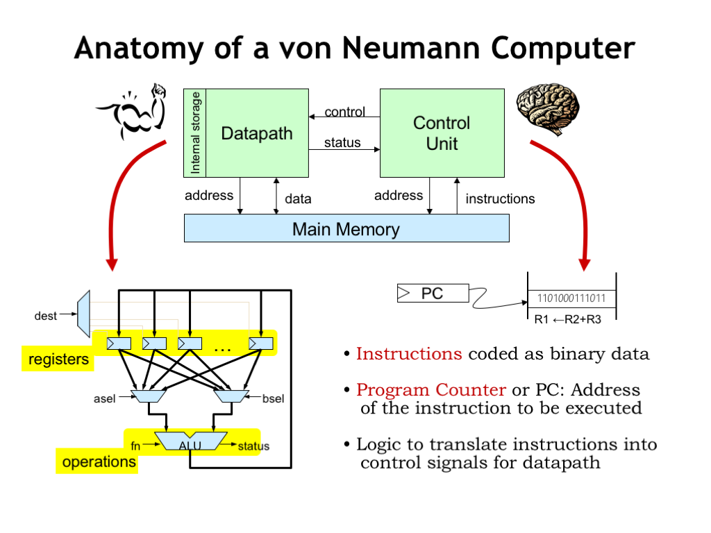
So this is the digital system we’ll build to perform computations. We’ll start with a datapath that contains some number of registers to hold data values. We’ll be able to select which registers will supply operands for the arithmetic and logic unit that will perform an operation. The ALU produces a result and other status signals. The ALU result can be written back to one of the registers for later use. We’ll provide the datapath with means to move data to and from main memory.
There will be a control unit that provides the necessary control signals to the datapath. In the example datapath shown here, the control unit would provide ASEL and BSEL to select two register values as operands and DEST to select the register where the ALU result will be written. If the datapath had, say, 32 internal registers, ASEL, BSEL and DEST would be 5-bit values, each specifying a particular register number in the range 0 to 31. The control unit also provides the FN function code that controls the operation performed by the ALU. The ALU we designed in Part 1 of the course requires a 6-bit function code to select between a variety of arithmetic, boolean and shift operations.
The control unit would load values from main memory to be interpreted as instructions. The control unit contains a register, called the “program counter”, that keeps track of the address in main memory of the next instruction to be executed. The control unit also contains a (hopefully small) amount of logic to translate the instruction fields into the necessary control signals. Note the control unit receives status signals from the datapath that will enable programs to execute different sequences of instructions if, for example, a particular data value was zero.
The datapath serves as the brawn of our digital system and is responsible for storing and manipulating data values. The control unit serves as the brain of our system, interpreting the program stored in main memory and generating the necessary sequence of control signals for the datapath.
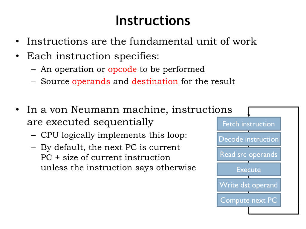
Instructions are the fundamental unit of work. They’re fetched by the control unit and executed one after another in the order they are fetched. Each instruction specifies the operation to be performed along with the registers to supply the source operands and destination register where the result will be stored.
In a von Neumann machine, instruction execution involves the steps shown here: the instruction is loaded from the memory location whose address is specified by the program counter. When the requested data is returned by the memory, the instruction fields are converted to the appropriate control signals for the datapath, selecting the source operands from the specified registers, directing the ALU to perform the specified operation, and storing the result in the specified destination register. The final step in executing an instruction is updating the value of the program counter to be the address of the next instruction.
This execution loop is performed again and again. Modern machines can execute more than a billion instructions per second!
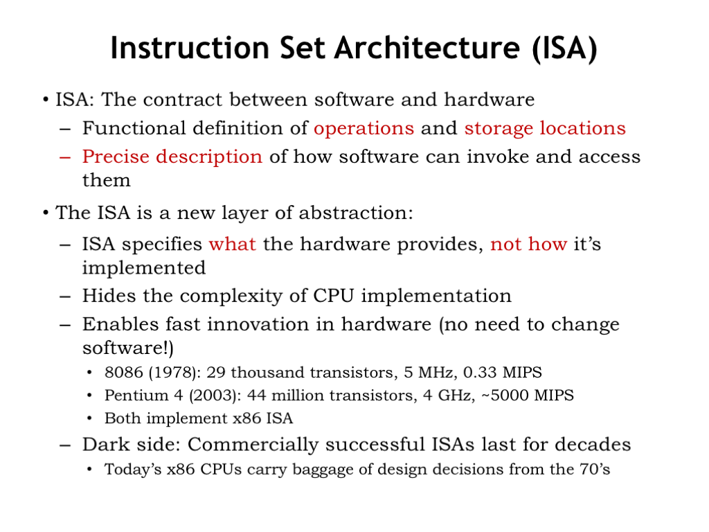
The discussion so far has been a bit abstract. Now it’s time to roll up our sleeves and figure out what instructions we want our system to support. The specification of instruction fields and their meaning along with the details of the datapath design are collectively called the instruction set architecture (ISA) of the system. The ISA is a detailed functional specification of the operations and storage mechanisms and serves as a contract between the designers of the digital hardware and the programmers who will write the programs. Since the programs are stored in main memory and can hence be changed, we’ll call them software, to distinguish them from the digital logic which, once implemented, doesn’t change. It’s the combination of hardware and software that determine the behavior of our system.
The ISA is a new layer of abstraction: we can write programs for the system without knowing the implementation details of the hardware. As hardware technology improves we can build faster systems without having to change the software. You can see here that over a fifteen year timespan, the hardware for executing the Intel x86 instruction set went from executing 300,000 instructions per second to executing 5 billion instructions per second. Same software as before, we’ve just taken advantage of smaller and faster MOSFETs to build more complex circuits and faster execution engines.
But a word of caution is in order! It’s tempting to make choices in the ISA that reflect the constraints of current technologies, e.g., the number of internal registers, the width of the operands, or the maximum size of main memory. But it will be hard to change the ISA when technology improves since there’s a powerful economic incentive to ensure that old software can run on new machines, which means that a particular ISA can live for decades and span many generations of technology. If your ISA is successful, you’ll have to live with any bad choices you made for a very long time.
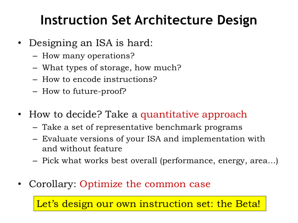
Designing an ISA is hard! What are the operations that should be supported? How many internal registers? How much main memory? Should we design the instruction encoding to minimize program size or to keep the logic in the control unit as simple as possible? Looking into our crystal ball, what can we say about the computation and storage capabilities of future technologies?
We’ll answer these questions by taking a quantitative approach. First we’ll choose a set of benchmark programs, chosen as representative of the many types of programs we expect to run on our system. So some benchmark programs will perform scientific and engineering computations, some will manipulate large data sets or perform database operations, some will require specialized computations for graphics or communications, and so on. Happily, after many decades of computer use, several standardized benchmark suites are available for us to use.
We’ll then implement the benchmark programs using our instruction set and simulate their execution on our proposed datapath. We’ll evaluate the results to measure how well the system performs. But what do we mean by “well”? That’s where it gets interesting: “well” could refer to execution speed, energy consumption, circuit size, system cost, etc. If you’re designing a smart watch, you’ll make different choices than if you’re designing a high-performance graphics card or a data-center server.
Whatever metric you choose to evaluate your proposed system, there’s an important design principle we can follow: identify the common operations and focus on them as you optimize your design. For example, in general-purpose computing, almost all programs spend a lot of their time on simple arithmetic operations and accessing values in main memory. So those operations should be made as fast and energy efficient as possible.
Now, let’s get to work designing our own instruction set and execution engine, a system we’ll call the Beta.
The Beta is an example of a reduced-instruction-set computer (RISC) architecture. “Reduced” refers to the fact that in the Beta ISA, most instructions only access the internal registers for their operands and destination. Memory values are loaded and stored using separate memory-access instructions, which implement only a simple address calculation. These reductions lead to smaller, higher-performance hardware implementations and simpler compilers on the software side. The ARM and MIPS ISAs are other examples of RISC architectures. Intel’s x86 ISA is more complex.
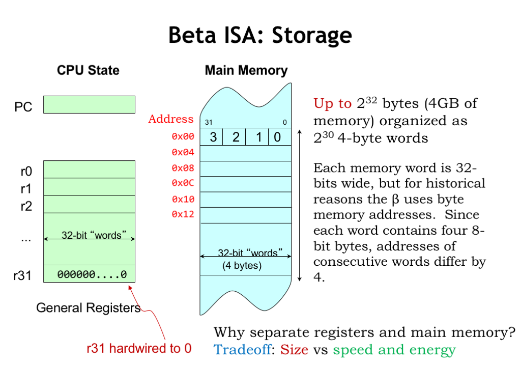
There is a limited amount of storage inside of the CPU — using the language of sequential logic, we’ll refer to this as the CPU state. There’s a 32-bit program counter (PC for short) that holds the address of the current instruction in main memory. And there are thirty-two registers, numbered 0 through 31. Each register holds a 32-bit value. We’ll use use 5-bit fields in the instruction to specify the number of the register to be used an operand or destination. As shorthand, we’ll refer to a register using the prefix “R” followed by its number, e.g., “R0” refers to the register selected by the 5-bit field 0b00000.
Register 31 (R31) is special — its value always reads as 0 and writes to R31 have no affect on its value.
The number of bits in each register and hence the number of bits supported by ALU operations is a fundamental parameter of the ISA. The Beta is a 32-bit architecture. Many modern computers are 64-bit architectures, meaning they have 64-bit registers and a 64-bit datapath.
Main memory is an array of 32-bit words. Each word contains four 8-bit bytes. The bytes are numbered 0 through 3, with byte 0 corresponding to the low-order 7 bits of the 32-bit value, and so on. The Beta ISA only supports word accesses, either loading or storing full 32-bit words. Most “real” computers also support accesses to bytes and half-words.
Even though the Beta only accesses full words, following a convention used by many ISAs it uses byte addresses. Since there are 4 bytes in each word, consecutive words in memory have addresses that differ by 4. So the first word in memory has address 0, the second word address 4, and so on. You can see the addresses to left of each memory location in the diagram shown here. Note that we’ll usually use hexadecimal notation when specifying addresses and other binary values — the “0x” prefix indicates when a number is in hex. When drawing a memory diagram, we’ll follow the convention that addresses increase as you read from top to bottom.
The Beta ISA supports 32-bit byte addressing, so an address fits exactly into one 32-bit register or memory location. The maximum memory size is \(2^{32}\) bytes or \(2^{30}\) words — that’s 4 gigabytes (4 GB) or one billion words of main memory. Some Beta implementations might actually have a smaller main memory, i.e., one with fewer than 1 billion locations.
Why have separate registers and main memory? Well, modern programs and datasets are very large, so we’ll want to have a large main memory to hold everything. But large memories are slow and usually only support access to one location at a time, so they don’t make good storage for use in each instruction which needs to access several operands and store a result. If we used only one large storage array, then an instruction would need to have three 32-bit addresses to specify the two source operands and destination — each instruction encoding would be huge! And the required memory accesses would have to be one-after-the-other, really slowing down instruction execution.
On the other hand, if we use registers to hold the operands and serve as the destination, we can design the register hardware for parallel access and make it very fast. To keep the speed up we won’t be able to have very many registers — a classic size-vs-speed performance tradeoff we see in digital systems all the time. In the end, the tradeoff leading to the best performance is to have a small number of very fast registers used by most instructions and a large but slow main memory. So that’s what the BETA ISA does.
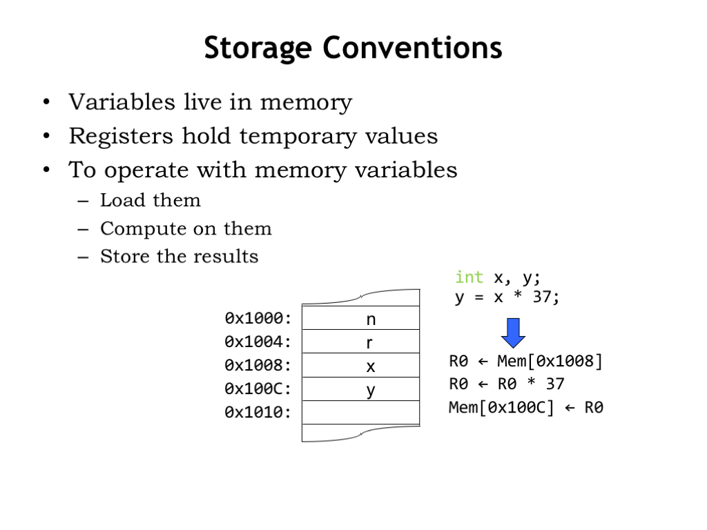
In general, all program data will reside in main memory. Each variable used by the program “lives” in a specific main memory location and so has a specific memory address. For example, in the diagram below, the value of variable “x” is stored in memory location 0x1008, and the value of “y” is stored in memory location 0x100C, and so on.
To perform a computation, e.g., to compute x*37 and store the result in y, we would have to first load the value of x into a register, say, R0. Then we would have the datapath multiply the value in R0 by 37, storing the result back into R0. Here we’ve assumed that the constant 37 is somehow available to the datapath and doesn’t itself need to be loaded from memory. Finally, we would write the updated value in R0 back into memory at the location for y.
Whew! A lot of steps… Of course, we could avoid all the loading and storing if we chose to keep the values for x and y in registers. Since there are only 32 registers, we can’t do this for all of our variables, but maybe we could arrange to load x and y into registers, do all the required computations involving x and y by referring to those registers, and then, when we’re done, store changes to x and y back into memory for later use. Optimizing performance by keeping often-used values in registers is a favorite trick of programmers and compiler writers.
So the basic program template is some loads to bring values into the registers, followed by computation, followed by any necessary stores. ISAs that use this template are usually referred to as “load-store architectures”.
Having talked about the storage resources provided by the Beta ISA, let’s design the Beta instructions themselves. This might be a good time to print a copy of the handout called the “Summary of Beta Instruction Formats” so you’ll have it for handy reference.
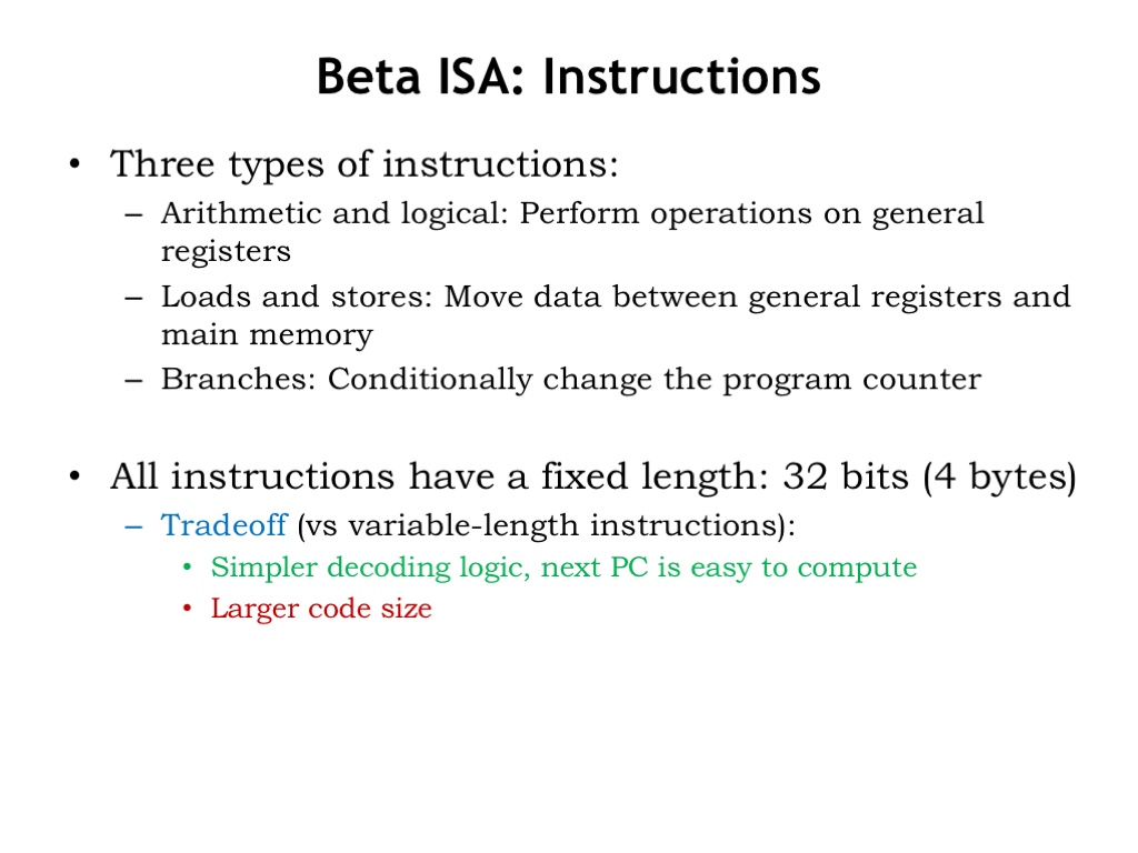
The Beta has three types of instructions: compute instructions that perform arithmetic and logic operations on register values, load and store instructions that access values in main memory, and branch instructions that change the value of the program counter.
We’ll discuss each class of instructions in turn.
In the Beta ISA, all the instruction encodings are the same size: each instruction is encoded in 32 bits and hence occupies exactly one 32-bit word in main memory. This instruction encoding leads to simpler control-unit logic for decoding instructions. And computing the next value of the program counter is very simple: for most instructions, the next instruction can be found in the following memory location. We just need to add 4 to the current value of program counter to advance to the next instruction.
As we saw in Part 1 of the course, fixed-length encodings are often inefficient in the sense that the same information content (in this case, the encoded program) can be encoded using fewer bits. To do better we would need a variable-length encoding for instructions, where frequently-occurring instructions would use a shorter encoding. But hardware to decode variable-length instructions is complex since there may be several instructions packed into one memory word, while other instructions might require loading several memory words. The details can be worked out, but there’s a performance and energy cost associated with the more efficient encoding.
Nowadays, advances in memory technology have made memory size less of an issue and the focus is on the higher-performance needed by today’s applications. Our choice of a fixed-length encoding leads to larger code size, but keeps the hardware execution engine small and fast.
The computation performed by the Beta datapath happens in the arithmetic-and-logic unit (ALU). We’ll be using the ALU designed in Part 1 of the course.
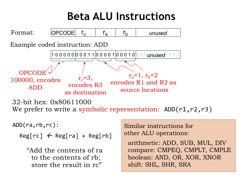
The Beta ALU instructions have 4 instruction fields. There’s a 6-bit field specifying the ALU operation to be performed — this field is called the opcode. The two source operands come from registers whose numbers are specified by the 5-bit “ra” and “rb” fields. So we can specify any register from R0 to R31 as a source operand. The destination register is specified by the 5-bit “rc” field.
This instruction format uses 21 bits of the 32-bit word, the remaining bits are unused and should be set to 0. The diagram shows how the fields are positioned in the 32-bit word. The choice of position for each field is somewhat arbitrary, but to keep the hardware simple, when we can we’ll want to use the same field positions for similar fields in the other instruction encodings. For example, the opcode will always be found in bits [31:26] of the instruction.
Here’s the binary encoding of an ADD instruction. The opcode for ADD is the 6-bit binary value 0b100000 — you can find the binary for each opcode in the Opcode Table in the handout mentioned before. The “rc” field specifies that the result of the ADD will be written into R3. And the “ra” and “rb” fields specify that the first and second source operands are R1 and R2 respectively. So this instruction adds the 32-bit values found in R1 and R2, writing the 32-bit sum into R3.
Note that it’s permissible to refer to a particular register several times in the same instruction. So, for example, we could specify R1 as the register for both source operands AND also as the destination register. If we did, we’d be adding R1 to R1 and writing the result back into R1, which would effectively multiply the value in R1 by 2.
Since it’s tedious and error-prone to transcribe 32-bit binary values, we’ll often use hexadecimal notation for the binary representation of an instruction. In this example, the hexadecimal notation for the encoded instruction is 0x80611000. However, it’s *much* easier if we describe the instructions using a functional notation, e.g., “ADD(r1,r2,r3)”. Here we use a symbolic name for each operation, called a mnemonic. For this instruction the mnemonic is “ADD”, followed by a parenthesized list of operands, in this case the two source operands (r1 and r2), then the destination (r3). So we’ll understand that ADD(ra,rb,rc) is shorthand for asking the Beta to compute the sum of the values in registers ra and rb, writing the result as the new value of register rc.
Here’s the list of the mnemonics for all the operations supported by the Beta. There is a detailed description of what each instruction does in the Beta Documentation handout. Note that all these instructions use same 4-field template, differing only in the value of the opcode field. This first step was pretty straightforward — we simply provided instruction encodings for the basic operations provided by the ALU.
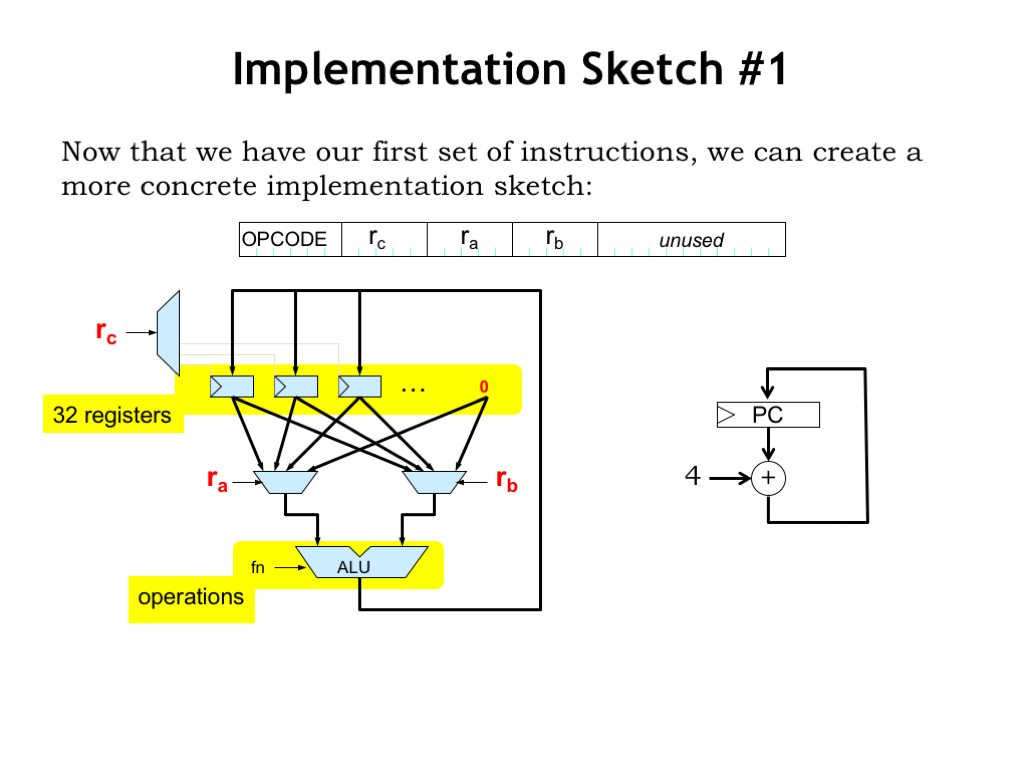
Now that we have our first group of instructions, we can create a more concrete implementation sketch.
Here we see our proposed datapath. The 5-bit “ra” and “rb” fields from the instruction are used to select which of the 32 registers will be used for the two operands. Note that register 31 isn’t actually a read/write register, it’s just the 32-bit constant 0, so that selecting R31 as an operand results in using the value 0. The 5-bit “rc” field from the instruction selects which register will be written with the result from the ALU. Not shown is the hardware needed to translate the instruction opcode to the appropriate ALU function code — perhaps a 64-location ROM could be used to perform the translation by table lookup.
The program counter logic supports simple sequential execution of instructions. It’s a 32-bit register whose value is updated at the end of each instruction by adding 4 to its current value. This means the next instruction will come from the memory location following the one that holds the current instruction.
In this diagram we see one of the benefits of a RISC architecture: there’s not much logic needed to decode the instruction to produce the signals needed to control the datapath. In fact, many of the instruction fields are used as-is!
ISA designers receive many requests for what are affectionately known as “features” — additional instructions that, in theory, will make the ISA better in some way. Dealing with such requests is the moment to apply our quantitative approach in order to be able to judge the tradeoffs between cost and benefits.
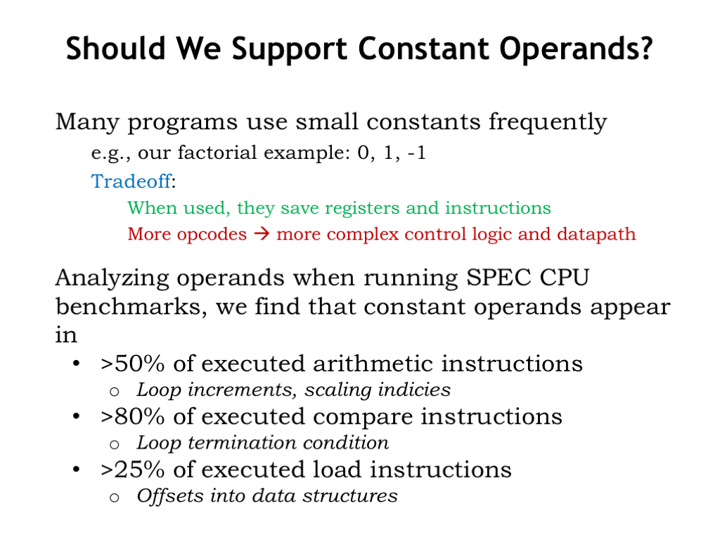
Our first “feature request” is to allow small constants as the second operand in ALU instructions. So if we replaced the 5-bit “rb” field, we would have room in the instruction to include a 16-bit constant as bits [15:0] of the instruction. The argument in favor of this request is that small constants appear frequently in many programs and it would make programs shorter if we didn’t have use load operations to read constant values from main memory. The argument against the request is that we would need additional control and datapath logic to implement the feature, increasing the hardware cost and probably decreasing the performance.
So our strategy is to modify our benchmark programs to use the ISA augmented with this feature and measure the impact on a simulated execution. Looking at the results, we find that there is compelling evidence that small constants are indeed very common as the second operands to many operations. Note that we’re not so much interested in simply looking at the code. Instead we want to look at what instructions actually get executed while running the benchmark programs. This will take into account that instructions executed during each iteration of a loop might get executed 1000’s of times even though they only appear in the program once.
Looking at the results, we see that over half of the arithmetic instructions have a small constant as their second operand.
Comparisons involve small constants 80% of the time. This probably reflects the fact that during execution comparisons are used in determining whether we’ve reached the end of a loop.
And small constants are often found in address calculations done by load and store operations.
Operations involving constant operands are clearly a common case, one well worth optimizing. Adding support for small constant operands to the ISA resulted in programs that were measurably smaller and faster. So: feature request approved!
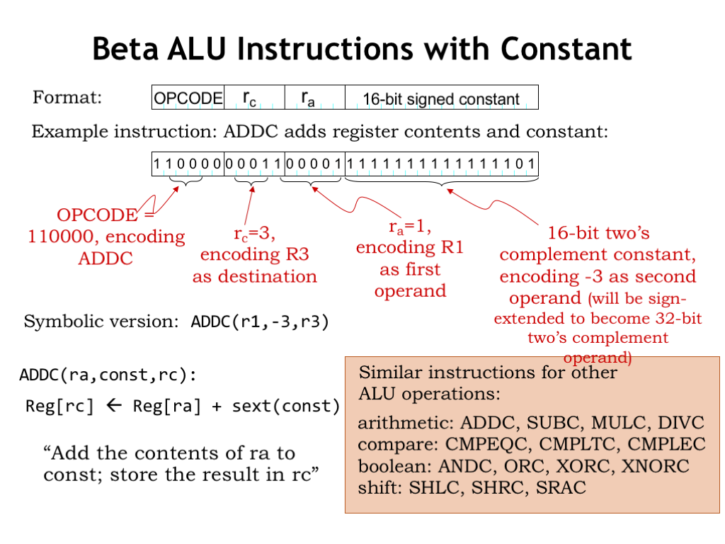
Here we see the second of the two Beta instruction formats. It’s a modification of the first format where we’ve replaced the 5-bit “rb” field with a 16-bit field holding a constant in two’s complement format. This will allow us to represent constant operands in the range of 0x8000 (decimal -32768) to 0x7FFF (decimal 32767).
Here’s an example of the add-constant (ADDC) instruction which adds the contents of R1 and the constant -3, writing the result into R3. We can see that the second operand in the symbolic representation is now a constant (or, more generally, an expression that can evaluated to get a constant value).
One technical detail needs discussion: the instruction contains a 16-bit constant, but the datapath requires a 32-bit operand. How does the datapath hardware go about converting from, say, the 16-bit representation of -3 to the 32-bit representation of -3?
Comparing the 16-bit and 32-bit representations for various constants, we see that if the 16-bit two’s-complement constant is negative (i.e., its high-order bit is 1), the high sixteen bits of the equivalent 32-bit constant are all 1’s. And if the 16-bit constant is non-negative (i.e., its high-order bit is 0), the high sixteen bits of the 32-bit constant are all 0’s. Thus the operation the hardware needs to perform is “sign extension” where the sign-bit of the 16-bit constant is replicated sixteen times to form the high half of the 32-constant. The low half of the 32-bit constant is simply the 16-bit constant from the instruction. No additional logic gates will be needed to implement sign extension — we can do it all with wiring.
Here are the fourteen ALU instructions in their “with constant” form, showing the same instruction mnemonics but with a “C” suffix indicate the second operand is a constant. Since these are additional instructions, these have different opcodes than the original ALU instructions.
Finally, note that if we need a constant operand whose representation does NOT fit into 16 bits, then we have to store the constant as a 32-bit value in a main memory location and load it into a register for use just like we would any variable value.
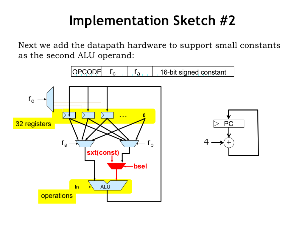
To give some sense for the additional datapath hardware that will be needed, let’s update our implementation sketch to add support for constants as the second ALU operand. We don’t have to add much hardware: just a multiplexer which selects either the “rb” register value or the sign-extended constant from the 16-bit field in the instruction. The BSEL control signal that controls the multiplexer is 1 for the ALU-with-constant instructions and 0 for the regular ALU instructions.
We’ll put the hardware implementation details aside for now and revisit them in a few lectures.
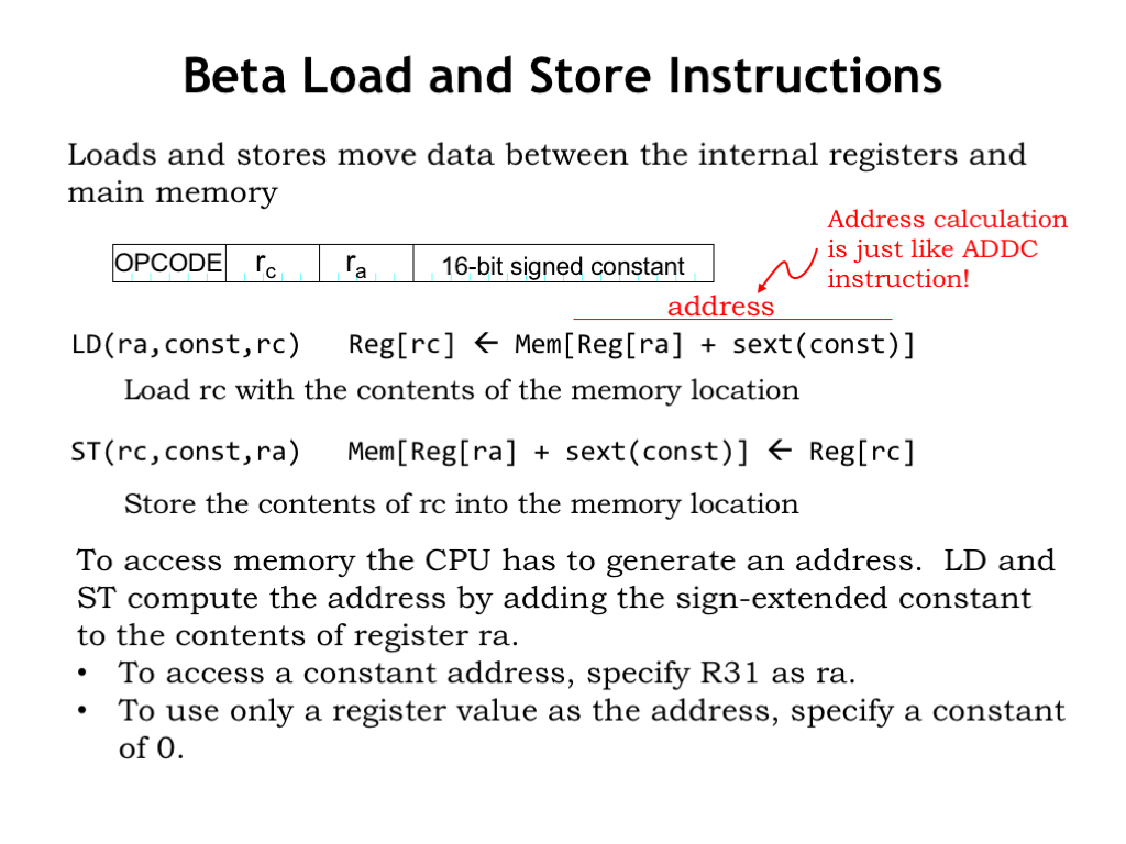
Now let’s turn our attention to the second class of instructions: load (LD) and store (ST), which allow the CPU to access values in memory. Note that since the Beta is a load-store architecture these instructions are the *only* mechanism for accessing memory values.
The LD and ST instructions use the same instruction template as the ALU-with-constant instructions. To access memory, we’ll need a memory address, which is computed by adding the value of the “ra” register to the sign-extended 16-bit constant from the low-order 16 bits of the instruction. This computation is exactly the one performed by the ADDC instruction — so we’ll reuse that hardware — and the sum is sent to main memory as the byte address of the location to be accessed. For the LD instruction, the data returned by main memory is written to the “rc” register.
The store instruction (ST) performs the same address calculation as LD, then reads the data value from the “rc” register and sends both to main memory. The ST instruction is special in several ways: it’s the only instruction that needs to read the value of the “rc” register, so we’ll need to adjust the datapath hardware slightly to accommodate that need. And since “rc” is serving as a source operand, it appears as the first operand in the symbolic form of the instruction, followed by “const” and “ra” which are specifying the destination address. ST is the only instruction that does *not* write a result into the register file at end of the instruction.
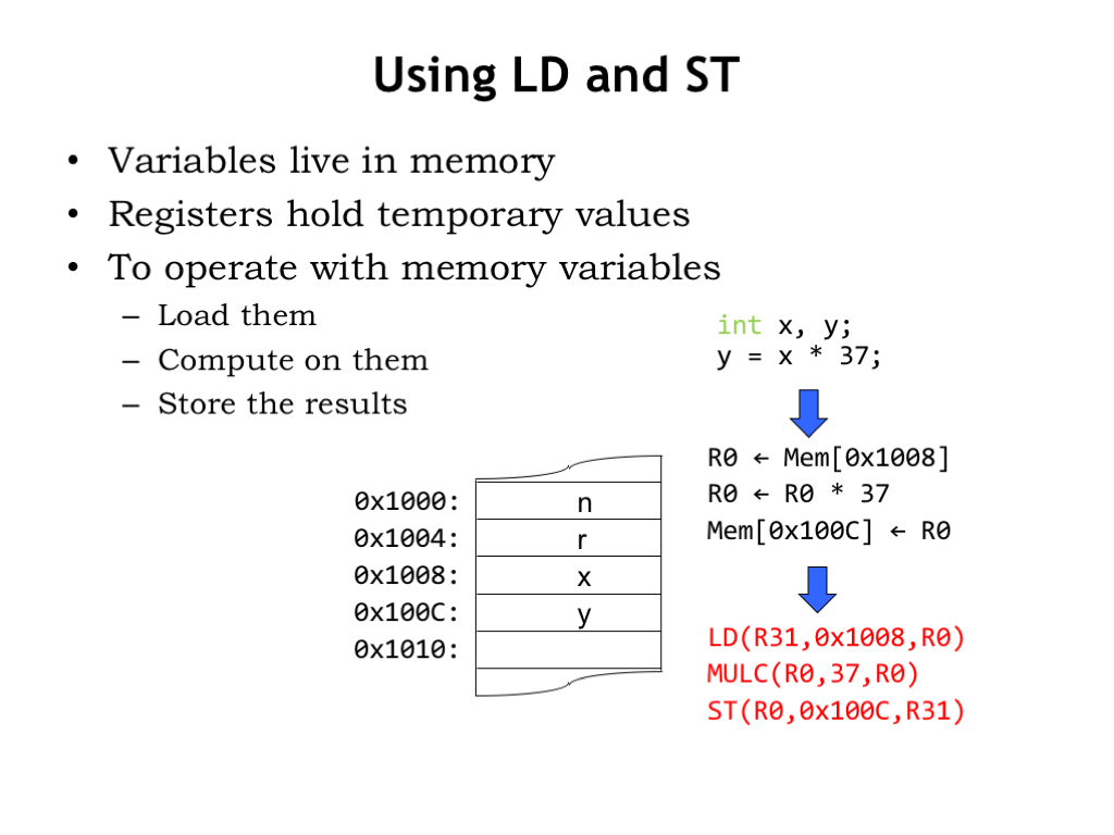
Here’s the example we saw earlier, where we needed to load the value of the variable x from memory, multiply it by 37 and write the result back to the memory location that holds the value of the variable y.
Now that we have actual Beta instructions, we’ve expressed the computation as a sequence of three instructions. To access the value of variable x, the LD instruction adds the contents of R31 to the constant 0x1008, which sums to 0x1008, the address we need to access. The ST instruction specifies a similar address calculation to write into the location for the variable y.
The address calculation performed by LD and ST works well when the locations we need to access have addresses that fit into the 16-bit constant field. What happens when we need to access locations at addresses higher than 0x7FFF? Then we need to treat those addresses as we would any large constant, and store those large addresses in main memory so they can be loaded into a register to be used by LD and ST. Okay, but what if the number of large constants we need to store is greater than will fit in low memory, i.e., the addresses we can access directly? To solve this problem, the Beta includes a “load relative” (LDR) instruction, which we’ll see in the lecture on the Beta implementation.
Finally, let’s discuss the third class of instructions that let us change the program counter. Up until now, the program counter has simply been incremented by 4 at the end of each instruction, so that the next instruction comes from the memory location that immediately follows the location that held the current instruction, i.e., the Beta has been executing instructions sequentially from memory.
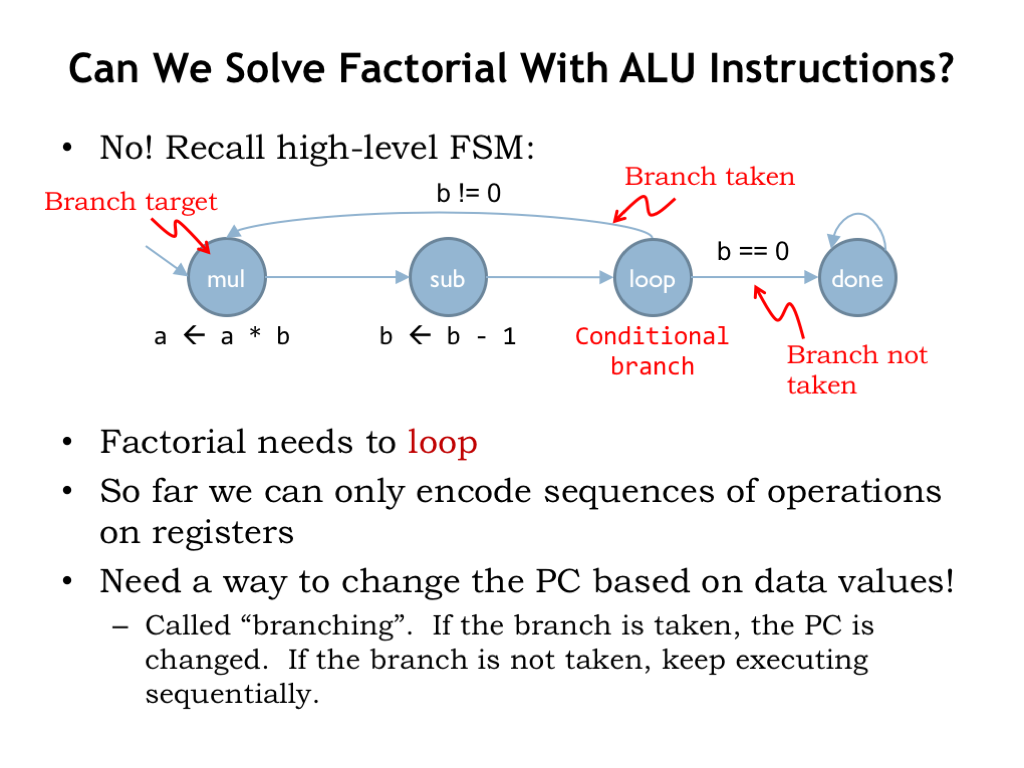
But in many programs, such as in factorial, we need to disrupt sequential execution, either to loop back to repeat some earlier instruction, or to skip over instructions because of some data dependency. We need a way to change the program counter based on data values generated by the program’s execution. In the factorial example, as long as b is not equal to 0, we need to keep executing the instructions that calculate a*b and decrement b. So we need instructions to test the value of b after it’s been decremented and if it’s non-zero, change the PC to repeat the loop one more time.
Changing the PC depending on some condition is implemented by a branch instruction, and the operation is referred to as a “conditional branch”. When the branch is taken, the PC is changed and execution is restarted at the new location, which is called the branch target. If the branch is not taken, the PC is incremented by 4 and execution continues with the instruction following the branch.
As the name implies, a branch instruction represents a potential fork in the execution sequence. We’ll use branches to implement many different types of control structures: loops, conditionals, procedure calls, etc.
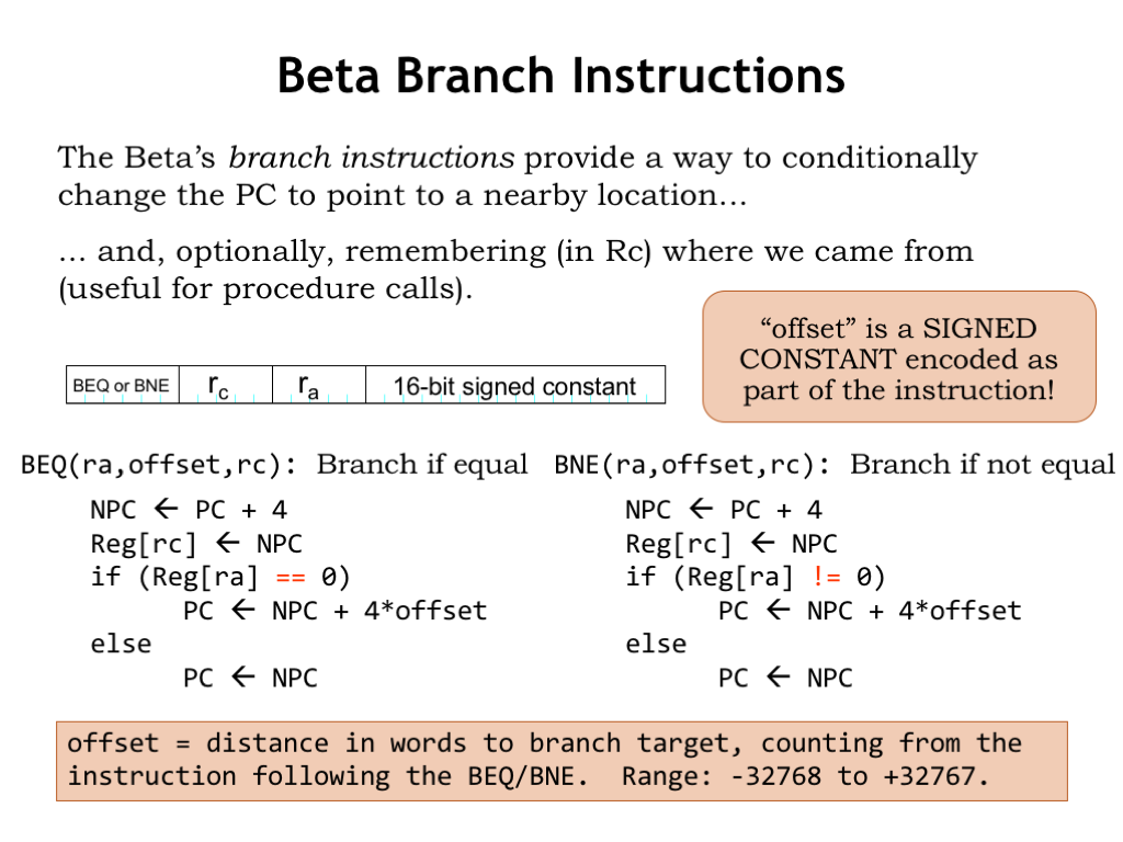
Branch instructions also use the instruction format with the 16-bit signed constant. The operation of the branch instructions are a bit complicated, so let’s walk through their operation step-by-step.
Let’s start by looking at the operation of the BEQ instruction. First the usual PC+4 calculation is performed, giving us the address of the instruction following the BEQ. This value is written to the “rc” register whether or not the branch is taken. This feature of branches is pretty handy and we’ll use it to implement procedure calls a couple of lectures from now. Note that if we don’t need to remember the PC+4 value, we can specify R31 as the “rc” register.
Next, BEQ tests the value of the “ra” register to see if it’s equal to 0. If it is equal to 0, the branch is taken and the PC is incremented by the amount specified in the constant field of the instruction. Actually the constant, called an offset since we’re using it to offset the PC, is treated as a word offset and is multiplied by 4 to convert it a byte offset since the PC uses byte addressing. If the contents of the “ra” register is not equal to 0, the PC is incremented by 4 and execution continues with the instruction following the BEQ.
Let me say a few more words about the offset. The branches are using what’s referred to as “pc-relative addressing”. That means the address of the branch target is specified relative to the address of the branch, or, actually, relative to the address of the instruction following the branch. So an offset of 0 would refer to the instruction following the branch and an offset of -1 would refer to the branch itself. Negative offsets are called “backwards branches” and are usually seen at branches used at the end of loops, where the looping condition is tested and we branch backwards to the beginning of the loop if another iteration is called for. Positive offsets are called “forward branches” and are usually seen in code for “if statements”, where we might skip over some part of the program if a condition is not true.
We can use BEQ to implement a so-called unconditional branch, i.e., a branch that is always taken. If we test R31 to see if it’s 0, that’s always true, so BEQ(R31,…) would always branch to the specified target.
There’s also a BNE instruction, identical to BEQ in its operation except the sense of the condition is reversed: the branch is taken if the value of register “ra” is non-zero.
It might seem that only testing for zero/non-zero doesn’t let us do everything we might want to do. For example, how would we branch if “a < b”? That’s where the compare instructions come in — they do more complicated comparisons, producing a non-zero value if the comparison is true and a zero value if the comparison is false. Then we can use BEQ and BNE to test the result of the comparison and branch appropriately.
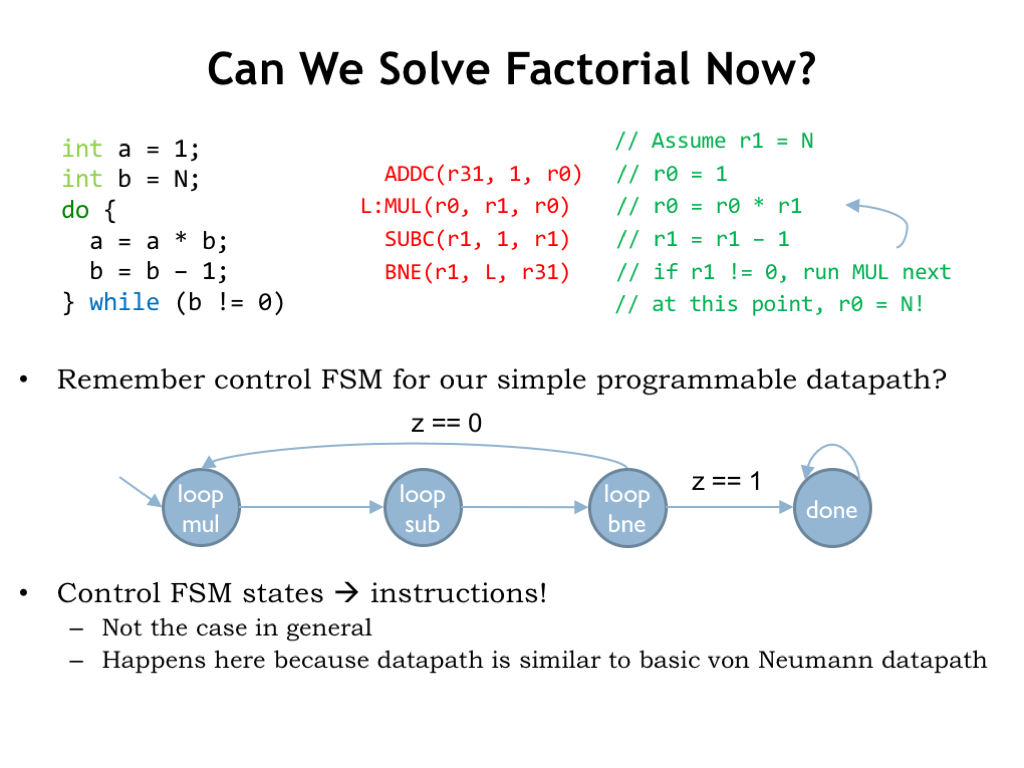
At long last we’re finally in a position to write Beta code to compute factorial using the iterative algorithm shown in C code on the left. In the Beta code, the loop starts at the second instruction and is marked with the “L:” label. The body of the loop consists of the required multiplication and the decrement of b. Then, in the fourth instruction, b is tested and, if it’s non-zero, the BNE will branch back to the instruction with the label L.
Note that in our symbolic notation for BEQ and BNE instructions we don’t write the offset directly since that would be a pain to calculate and would change if we added or removed instructions from the loop. Instead we reference the instruction to which we want to branch, and the program that translates the symbolic code into the binary instruction fields will do the offset calculation for us.
There’s a satisfying similarity between the Beta code and the operations specified by the high-level FSM we created for computing factorial in the simple programmable datapath discussed earlier in this lecture. In this example, each state in the high-level FSM matches up nicely with a particular Beta instruction. We wouldn’t expect that high degree of correspondence in general, but since our Beta datapath and the example datapath were very similar, the states and instructions match up pretty well.
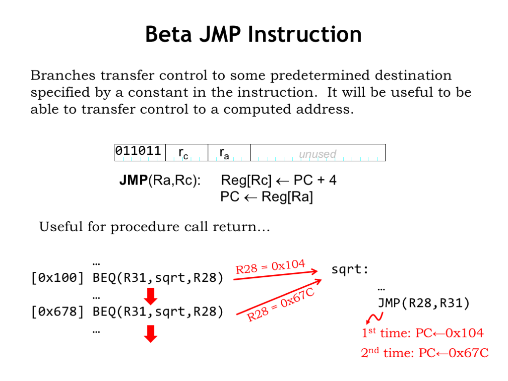
Finally, our last instruction! Branches conditionally transfer control to a specific target instruction. But we’ll also need the ability to compute the address of the target instruction — that ability is provided by the JMP instruction which simply sets the program counter to value from register “ra”. Like branches, JMP will write the PC+4 value into to the specified destination register.
This capability is very useful for implementing procedures in Beta code. Suppose we have a procedure “sqrt” that computes the square root of its argument, which is passed in, say, R0. We don’t show the code for sqrt on the right, except for the last instruction, which is a JMP.
On the left we see that the programmer wants to call the sqrt procedure from two different places in his program. Let’s watch what happens…
The first call to the sqrt procedure is implemented by the unconditional branch at location 0x100 in main memory. The branch target is the first instruction of the sqrt procedure, so execution continues there. The BEQ also writes the address of the following instruction (0x104) into its destination register, R28. When we reach the end of first procedure call, the JMP instruction loads the value in R28, which is 0x104, into the PC, so execution continues with the instruction following the first BEQ. So we’ve managed to return from the procedure and continue execution where we left off in the main program.
When we get to the second call to the sqrt procedure, the sequence of events is the same as before except that this time R28 contains 0x67C, the address of the instruction following the second BEQ. So the second time we reach the end of the sqrt procedure, the JMP sets the PC to 0x67C and execution resumes with the instruction following the second procedure call.
Neat! The BEQs and JMP have worked together to implement procedure call and return. We’ll discuss the implementation of procedures in detail in an upcoming lecture.
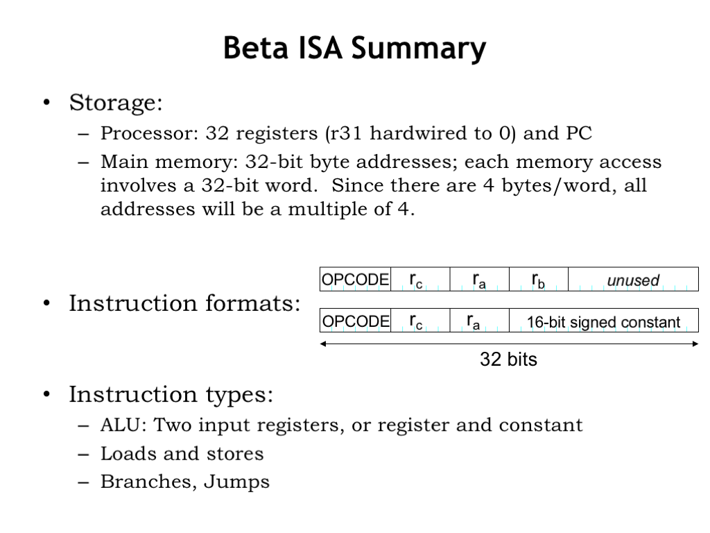
That wraps up the design of the Beta instruction set architecture. In summary, the Beta has 32 registers to hold values that can be used as operands for the ALU. All other values, along with the binary representation of the program itself, are stored in main memory. The Beta supports 32-bit memory addresses and can access values in \(2^{32} = 4\) gigabytes of main memory. All Beta memory access refer to 32-bit words, so all addresses will be a multiple of 4 since there are 4 bytes/word.
The are two instruction formats. The first specifies an opcode, two source registers and a destination register. The second replaces the second source register with a 32-bit constant, derived by sign-extending a 16-bit constant stored in the instruction itself.
There are three classes of instructions: ALU operations, LD and ST for accessing main memory, and branches and JMPs that change the order of execution.
And that’s it! As we’ll see in the next lecture, we’ll be able parlay this relatively simple repertoire of operations into a system that can execute any computation we can specify.


