
(a) Miller, et al. [1] noted the use of wafer curvature to infer stresses within thin films such as SOI. Derive the stress-curvature relationship given in Eq. 1, also known as the Stoney formula in the thin-film limit.
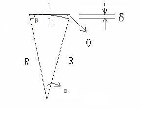
See the definitions of the symbols in Fig. 1, where l is the cantilever length. L is the arc length after bending, α is its corresponding center angle. θ is the angle between the original length and the bended length. R is the radius of the arch L. From the geometry
Relations we know:
θ + β = π/2
2 β + α = π
thus α = 2θ
On the other hand, in the right-angle triangle l L δ
l2 + δ2 = L2
In the limitation that δ<<L, θ = δ/L
The length of the arch L corresponds to an center angle of α by
α = L/R
thus κ = 1/R = α/L = 2θ/L = 2δ/L2 = 2δ/(l2 + δ2)
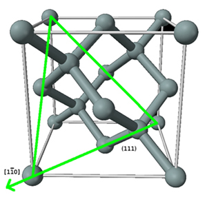
(b) Graphically represent the structure of Si in SOI, at the unit cell and micrometer-scale level, and separately indicate the closest packed plane and direction in that plane for this structure.
At the unit cell scale level, Si has diamond structure. The unit cell is FCC, with Si atoms filling half the tetrahedron interstitial sites. The closest packed plane is {111}, and the closest packed direction in this plane is plane is <110>.
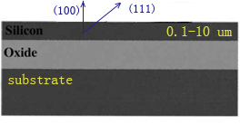
At micrometer-scale level, silicon thin film is single crystalline, with (100) oriented normal to the surface. SiO2 is amorphous. The substrate can be single silicon wafer, sapphire, etc.
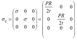
(c) During wafer bonding, blisters can occur at the wafer interfaces (Celler, Fig. 9 [2]). State the full tensorial stress state at the location of such a blister, and quantify the strains you would expect to correspond to this state in the adjacent Si.
Image removed due to copyright restrictions. Please see Fig. 9 in [2].
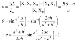
1. We use a sphere to simulate the blister as in Fig. 1.
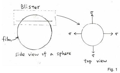
2. The stress within the film equals σ.
3. In the Smart Cut process, the thickness of the blister is relatively small compared to the radius of curvature of the blister. Therefore, we can use thin-wall approximation to approach this problem.
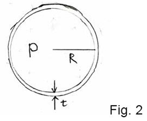
Stress:
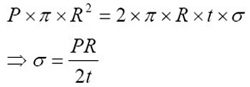
From Fig. 2,
P = pressure in the blister
R = radius of curvature of the blister
t = film thickness
4. Radius of curvature of the blister:
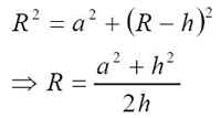
From Fig. 3,
a = radius of the circular base of the blister
h = height at the center of the blister
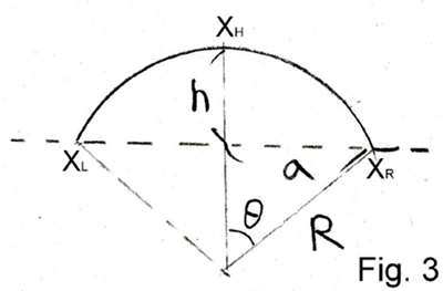
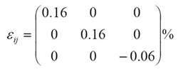
5. Strain:
Before forming a blister, the profile of the film is along XLXR in Fig. 3. However, after forming a blister, the film profile is along XLXHXR. Therefore, the length of film along x or y direction is stretched from |XLXR| to |XLXHXR|. As a result, the strain along x or y direction is
6. Stress state:
7. Strain state:
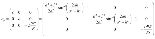
ν = Poisson’s ratio of the film
E = elastic modulus of the film
For instance, a = 1000 nm; h = 40 nm; ν = 0.16 [3]
References
[1] Miller, David C., Brad L. Boyce, Michael T. Dugger, Thomas E. Buchheit, and Ken Gall. “Characteristics of a Commercially Available Silicon-on-Insulator MEMS Materials.” Sensors and Actuators A 138 (2007): 130-144.
[2] Celler, G. K., and Sorin Cristoloveanu. “Frontiers of Silicon-on-Insulator.” Journal of Applied Physics 93 (May 1, 2003): 4955-4978.
[3] Piatkowska, A., G. Gawlik, and J. Jagielski. “AFM Studies of Hydrogen Implanted Silicon.” Applied Surface Science 141 (March 1999): 333-338.
Plasticity and fracture of microelectronic thin films/lines | Problem Set 2 | Problem Set 3 | Problem Set 5
Effects of multidimensional defects on III-V semiconductor mechanics
Defect nucleation in crystalline metals
Role of water in accelerated fracture of fiber optic glass
Carbon nanotube mechanics
Superelastic and superplastic alloys
Mechanical behavior of a virus
Effects of radiation on mechanical behavior of crystalline materials


