
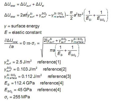
(b) Silicon on insulator delamination can be modeled by fracture between two dissimilar interfaces: Si and SiO2, for example. Assume that the interface blister you considered earlier is now an initial crack at the interface, and compute the fracture stress required to delaminate the film under Mode I loading. You can cite any required properties to implement a simple fracture theory such as Griffith’s.
Image removed due to copyright restrictions. Please see Fig. 9 in [5], with the dimensions a (width of the crack) and t (length of the crack) marked.
(c) In section 4 of the Frontiers paper [5], the authors discuss Bruel’s innovation as leading to the realization that fracture could be induced by shearing. What kind of mode of loading is this, and will the stress required to initiate fracture for a given material be lower in this mode than in Mode I?
The crack propagating in the direction normal to the shear stress, so the load is Mode III.
The stress required to initiate fracture for a given material will be higher in this mode than in Mode I. Mode I fracture is preceded only by linear elastic deformation. Mode III fracture is preceded by macroscopic yielding. The Gc values (fracture toughness) for Mode III fracture are typically higher than for Mode I and Mode II fracture as a result of increased crack tip blunting (which raises ρ) and greater values of ε.
References
[1] Tong, Q.-Y., Q. Gan, G. Hudson, G. Fountain, and P. Enquist. “Low-Temperature Hydrophobic Silicon Wafer Bonding.” Applied Physics Letters 83 (8 December 2003): 4767-4769.
[2] Asay, David B., and Seong H. Kim. “Effects of Adsorbed Water Layer Structure on Adhesion Force of Silicon Oxide Nanoasperity Contact in Humid Ambient.” Journal of Chemical Physics 124 (2006): 174712.
[3] Tu, Yuhai, and J. Tersoff. “Structure of the Silicon-Oxide Interface.” Thin Solid Films 400 (2001): 95-100.
[4] MatWeb.
[5] Celler, G. K., and Sorin Cristoloveanu. “Frontiers of Silicon-on-Insulator.” Journal of Applied Physics 93 (May 1, 2003): 4955-4978.
[6] Henley, F. J., and N. W. Cheung. “Method for Controlled Cleaving Process.” U.S. Patent No. 6,033,974.
[7] Courtney. Mechanical Behavior of Materials. 2nd ed. Long Grove, IL: Waveland Press Inc, 2005. ISBN: 9781577664253.
Plasticity and fracture of microelectronic thin films/lines | Problem Set 2 | Problem Set 3 | Problem Set 5
Effects of multidimensional defects on III-V semiconductor mechanics
Defect nucleation in crystalline metals
Role of water in accelerated fracture of fiber optic glass
Carbon nanotube mechanics
Superelastic and superplastic alloys
Mechanical behavior of a virus
Effects of radiation on mechanical behavior of crystalline materials


