
(b) Nejhad, et al. [1] present an analysis of retained internal stresses, and an associated elastic analysis in Eq. (8). Justify the form of Eq. (8) in terms of crystal structure of the two film materials of interest, and the origin of the strain terms.
Image removed due to copyright restrictions. Please see Fig. 7 in [1].
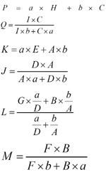
Let us consider the two-film structure model above; we can refer to ZnO as material 1, and Si3N4 as material 2.
And as shown by the paper, we have the table below:
Table removed due to copyright restrictions. Please see Table 1 in [1].
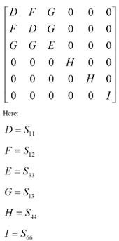
We can separate the compliance matrix to two parts: the first one is related to the 1, 2, 3 dimension, and the other is related to the 4, 5, 6 dimension below:
For Si3N4 as material 2,
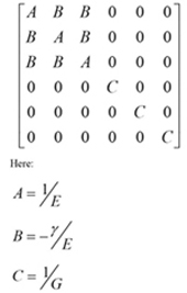
For ZnO as material 1,
For the two-layer composite, we can predict that the matrix has the below form,
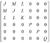
Now we need to determine P, Q, J, L, K and M from the matrices of materials 1 and 2. Let us determine them one by one.
We set the volume fraction of material 1 as a and the volume fraction of material 2 as b.The equation is shown below,
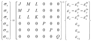
 = extrinsic strain = thermal strain in this work
 = intrinsic strain =
- dopants
- “atomic peening” which causes compressive stress
- microvoids which cause tensile stress
- gas entrapment which causes compressive stress
- shrinkage during process which causes tensile stress
- grain boundaries
(c) After Eq. (10) [1], the authors state that there are so many contributors of intrinsic strain that it is difficult to consider them quantitatively. Rank-order the sources they list in terms of relative amount of stress contribution for this system, and justify your answer.
The contributors of intrinsic strain mentioned in the literature are:
- dopants
- “atomic peening” which causes compressive stress
- microvoids which cause tensile stress
- gas entrapment which causes compressive stress
- shrinkage during process which causes tensile stress
- grain boundaries
For this system, the Si3N4 and ZnO films are deposited through PECVD.
Among the 6 contributors above;
- No dopants are introduced in the process of PECVD method, so this effect is very small.
- The “atomic peening” mechanism refers to the reflected neutral atoms bombarding the growing film at low sputtering pressures. The paper does not use sputtering method, so this effect is also small.
- Microvoids are caused by poor quality of film during process, which depends on the material, the environment, and the growth rate during PECVD.
- Since plasma (Ar, for example) is used in PECVD, it is very possible that gas will be entrapped in the film. Therefore this contribution is relatively significant.
- Shrinkage often happens in ceramics during sintering. There is no sintering in the process, so this contributor is small.
- For Si3N4, it is an amorphous film, so there are no grain boundaries. For ZnO, this effect is possible.
Integrating and rank-ordering all the effects, I get the conclusion below:
4 > 3 > 6 > 5 > 1 > 2
(d) Determine the % of residual stress in terms of the tensile and compressive failure strength of these two film materials. In other words, how closely does the residual stress in films or lines approach the failure stress of the bulk forms of these same materials?
Use the material properties give in Table I,
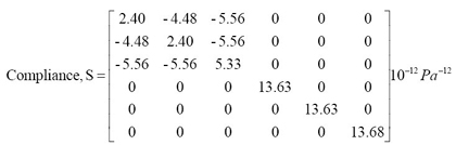
Given that residual strain is 10-12
Substituting S matrix and residual strain into the residual stress tensor equation given above, we have residual stress,
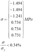
Provided yield stress of silicon nitride and zinc oxide is 900 and 412 MPa respectively.
Therefore, the residual stress is very small compared to the yield stress of silicon nitride or zinc oxide.
Reference
[1] Ghasemi-Nejhad, Mehrdad N., Chiling Pan, and Hongwei Feng. “Intrinsic Strain Modeling and Residual Stress Analysis for Thin-Film Processing of Layered Structures.” Journal of Electronic Packaging 125 (March 2003): 4-17.
Plasticity and fracture of microelectronic thin films/lines | Problem Set 2 | Problem Set 3 | Problem Set 5
Effects of multidimensional defects on III-V semiconductor mechanics
Defect nucleation in crystalline metals
Role of water in accelerated fracture of fiber optic glass
Carbon nanotube mechanics
Superelastic and superplastic alloys
Mechanical behavior of a virus
Effects of radiation on mechanical behavior of crystalline materials


