
6-152jf05.jpg
Description:
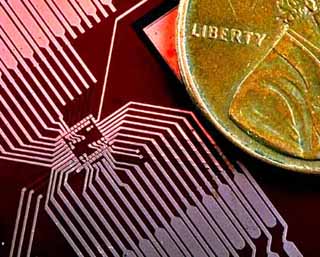
A device pad structure, shown with a penny for scale. (Image courtesy of Georgia Tech Center for Low Cost Electronics Packaging Research; photo by Stanley F. Leary. Image provided by the National Science Foundation Image Library.)
file
68 kB
6-152jf05.jpg
Alt text:
Photo showing a pad structure with a penny on top.
Caption:
A device pad structure, shown with a penny for scale. (Image courtesy of Georgia Tech Center for Low Cost Electronics Packaging Research; photo by Stanley F. Leary. Image provided by the National Science Foundation Image Library.)
Course Info
Instructors
As Taught In
Fall
2005
Level
Learning Resource Types
grading
Exam Solutions
grading
Exams
notes
Lecture Notes
assignment_turned_in
Problem Set Solutions
assignment
Problem Sets


