
L20: System-level communication
- Computer System Technologies
- Interfaces Last Forever
- System Interfaces & Modularity
- Buses, Interconnect, So…?
- Electrical Model for Real Wires
- Real-world Consequences
- Space & Time Constraints
- Gates, Wires, & Delays
- Interface Standard: Backplane Bus
- A Parallel Bus Transaction
- Bus Lines as Transmission Lines
- Meanwhile, Outside the Box…
- Lessons learned: Single driver; point-to-point
- Lessons learned: Clock recovery
- Serial, Point-to-point Communications
- Improving on the Bus
- Communications in Today’s Computers
- Example serial link: PCI Express (PCIe)
- Communication Topologies
- Quadratic-cost Topologies
- Mesh Topologies
- Logarithmic-latency Networks
- Communication Technologies: Latency
- Communications Futures
Content of the following slides is described in the surrounding text.
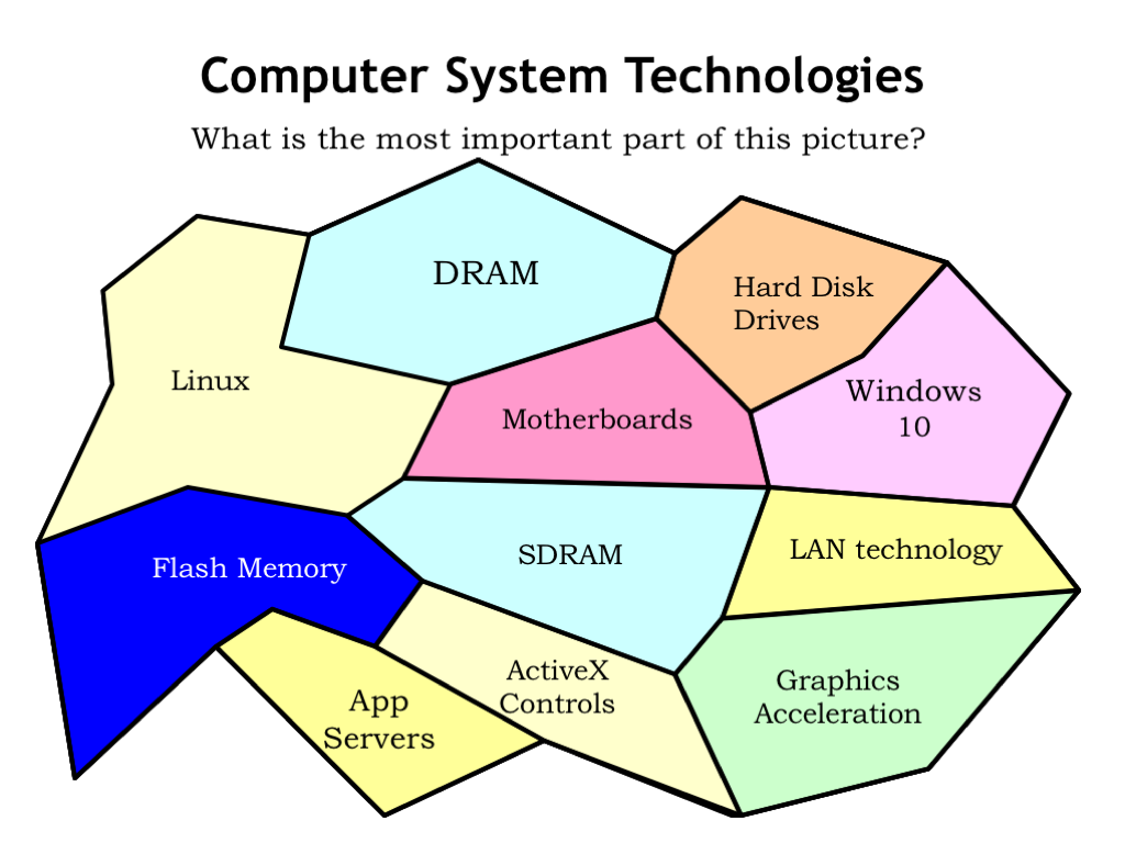
Computer systems bring together many technologies and harness them to provide fast execution of programs. Some of these technologies are relatively new, others have been with us for decades. Each of the system components comes with a detailed specification of their functionality and interface. The expectation is that system designers can engineer the system based on the component specifications without having to know the details of the implementations of each component. This is good since many of the underlying technologies change, often in ways that allow the components to become smaller, faster, cheaper, more energy efficient, and so on. Assuming the new components still implement same interfaces, they can be integrated into the system with very little effort.
The moral of this story is that the important part of the system architecture is the interfaces.
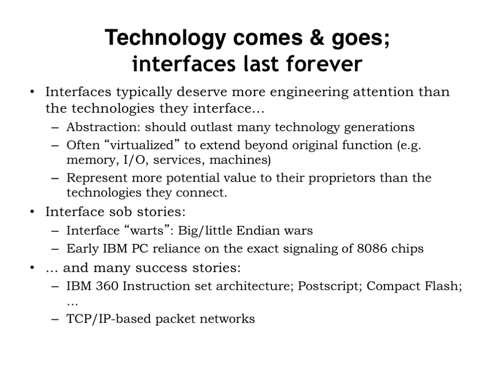
Our goal is to design interface specifications that can survive many generations of technological change. One approach to long-term survival is to base the specification on a useful abstraction that hides most, if not all, of the low-level implementation details. Operating systems provide many interfaces that have remained stable for many years. For example, network interfaces that reliably deliver streams of bytes to named hosts, hiding the details of packets, sockets, error detection and recovery, etc. Or windowing and graphics systems that render complex images, shielding the application from details about the underlying graphics engine. Or journaled file systems that behind-the-scenes defend against corruption in the secondary storage arrays.
Basically, we’re long since past the point where we can afford to start from scratch each time the integrated circuit gurus are able to double the number of transistors on a chip, or the communication wizards figure out how to go from 1GHz networks to 10GHz networks, or the memory mavens are able to increase the size of main memory by a factor of 4. The interfaces that insulate us from technological change are critical to ensure that improved technology isn’t a constant source of disruption.
There are some famous examples of where an apparently convenient choice of interface has had embarrassing long-term consequences. For example, back in the days of stand-alone computing, different ISAs made different choices on how to store multi-byte numeric values in main memory. IBM architectures are store the most-significant byte in the lowest address (so called “big endian”), while Intel’s x86 architectures store the least-significant byte first (so called “little endian”). But this leads to all sorts of complications in a networked world where numeric data is often transferred from system to system. This is a prime example of a locally-optimal choice having an unfortunate global impact. As the phrase goes: “a moment of convenience, a lifetime of regret.”
Another example is the system-level communication strategy chosen for the first IBM PC, the original personal computer based Intel CPU chips. IBM built their expansion bus for adding I/O peripherals, memory cards, etc., by simply using the interface signals provided by then-current x86 CPU. So the width of the data bus, the number of address pins, the data-transfer protocol, etc. where are exactly as designed for interfacing to that particular CPU. A logical choice since it got the job done while keeping costs as low a possible. But that choice quickly proved unfortunate as newer, higher-performance CPUs were introduced, capable of addressing more memory or providing 32-bit instead of 16-bit external data paths. So system architects were forced into offering customers the Hobson’s choice of crippling system throughput for the sake of backward compatibility, or discarding the networking card they bought last year since it was now incompatible with this year’s system.
But there are success stories too. The System/360 interfaces chosen by IBM in the early 1960s carried over to the System/370 in the 70’s and 80’s and to the Enterprise System Architecture/390 of the 90’s. Customers had the expectation that software written for the earlier machines would continue to work on the newer systems and IBM was able to fulfill that expectation.
Maybe the most notable long-term interface success is the design the TCP and IP network protocols in the early 70’s, which formed the basis for most packet-based network communication. A recent refresh expanded the network addresses from 32 to 128 bits, but that was largely invisible to applications using the network. It was a remarkably prescient set of engineering choices that stood the test of time for over four decades of exponential growth in network connectivity.
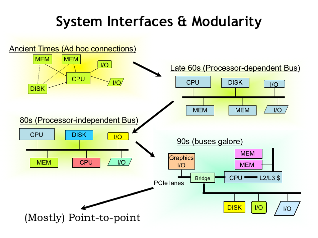
Today’s lecture topic is figuring out the appropriate interface choices for interconnecting system components. In the earliest systems these connections were very ad hoc in the sense that the protocols and physical implementation were chosen independently for each connection that had to be made. The cable connecting the CPU box to the memory box (yes, in those days, they lived in separate 19-inch racks!) was different than the cable connecting the CPU to the disk.
Improving circuit technologies allowed system components to shrink from cabinet-size to board-size and system engineers designed a modular packaging scheme that allowed users to mix-and-match board types that plugged into a communication backplane. The protocols and signals on the backplane reflected the different choices made by each vendor — IBM boards didn’t plug into Digital Equipment backplanes, and vice versa.
This evolved into some standardized communication backplanes that allowed users to do their own system integration, choosing different vendors for their CPU, memory, networking, etc. Healthy competition quickly brought prices down and drove innovation. However this promising development was overtaken by rapidly improving performance, which required communication bandwidths that simply could not be supported across a multi-board backplane.
These demands for higher performance and the ability to integrate many different communication channels into a single chip, lead to a proliferation of different channels. In many ways, the system architecture was reminiscent of the original systems — ad-hoc purpose-built communication channels specialized to a specific task.
As we’ll see, engineering considerations have led to the widespread adoption of general-purpose unidirectional point-to-point communication channels. There are still several types of channels depending on the required performance, the distance travelled, etc., but asynchronous point-to-point channels have mostly replaced the synchronous multi-signal channels of earlier systems.
Most system-level communications involve signaling over wires, so next we’ll look into some the engineering issues we’ve had to deal with as communication speeds have increased from kHz to GHz.
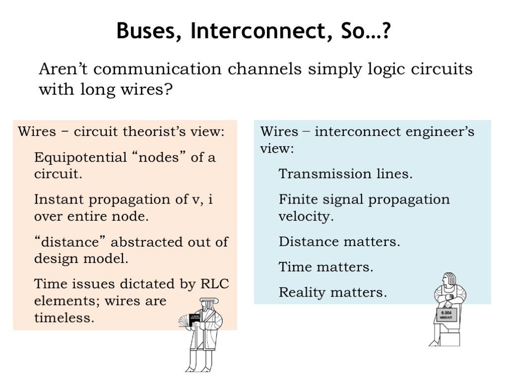
So, how hard can it be to build a communication channel? Aren’t they just logic circuits with a long wire that runs from one component to another?
A circuit theorist would tell you that wires in a schematic diagram are intended to represent the equipotential nodes of the circuit, which are used to connect component terminals. In this simple model, a wire has the same voltage at all points and any changes in the voltage or current at one component terminal is instantly propagated to the other component terminals connected to the same wire. The notion of distance is abstracted out of our circuit models: terminals are either connected by a wire, or they’re not. If there are resistances, capacitances, and inductances that need to be accounted for, the necessary components can be added to the circuit model. Wires are timeless. They are used to show how components connect, but they aren’t themselves components.
In fact, thinking of wires as equipotential nodes is a very workable model when the rate of change of the voltage on the wire is slow compared to the time it takes for an electromagnetic wave to propagate down the wire. Only as circuit speeds have increased with advances in integrated circuit technologies did this rule-of-thumb start to be violated in logic circuits where the components were separated by at most 10’s of inches.
In fact, it has been known since the late 1800s that changes in voltage levels take finite time to propagate down a wire. Oliver Heaviside was a self-taught English electrical engineer who, in the 1880’s, developed a set of “telegrapher’s equations” that described how signals propagate down wires. Using these, he was able to show how to improve the rate of transmission on then new transatlantic telegraph cable by a factor of 10.
We now know that for high-speed signaling we have to treat wires as transmission lines, which we’ll say more about in the next few slides. In this domain, the distance between components and hence the lengths of wires is of critical concern if we want to correctly predict the performance of our circuits. Distance and signal propagation matter — real-world wires are, in fact, fairly complex components!
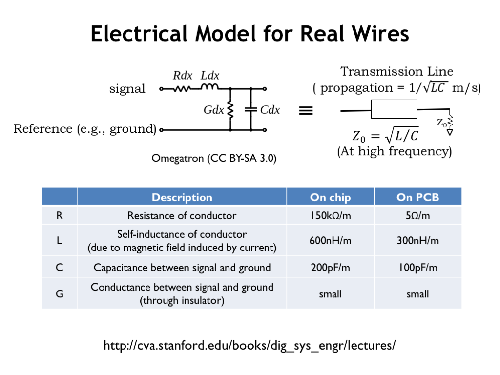
Here’s an electrical model for an infinitesimally small segment of a real-world wire. An actual wire is correctly modeled by imagining a many copies of the model shown here connected end-to-end. The signal, i.e., the voltage on the wire, is measured with respect to the reference node which is also shown in the model.
There are 4 parameters that characterize the behavior of the wire. R tells us the resistance of the conductor. It’s usually negligible for the wiring on printed circuit boards, but it can be significant for long wires in integrated circuits. L represents the self-inductance of the conductor, which characterizes how much energy will be absorbed by the wire’s magnetic fields when the current flowing through the wire changes. The conductor and reference node are separated by some sort insulator (which might be just air!) and hence form a capacitor with capacitance C. Finally, the conductance G represents the current that leaks through the insulator. Usually this is quite small.
The table shows the parameter values we might measure for wires inside an integrated circuit and on printed circuit boards.
If we analyze what happens when sending signals down the wire, we can describe the behavior of the wires using a single component called a transmission line which has a characteristic complex-valued impedance \(Z_0\). At high signaling frequencies and over the distances found on-chip or on circuit boards, such as one might find in a modern digital system, the transmission line is lossless, and voltage changes (“steps”) propagate down the wire at the rate of \(1/\sqrt(LC)\) meters per second. Using the values given here for a printed circuit board, the characteristic impedance is approximately 50 ohms and the speed of propagation is about 18 cm (7 in.) per ns.
To send digital information from one component to another, we change the voltage on the connecting wire, and that voltage step propagates from the sender to the receiver. We have to pay some attention to what happens to that energy front when it gets to the end of the wire! If we do nothing to absorb that energy, conservation laws tell us that it reflects off the end of the wire as an “echo” and soon our wire will be full of echoes from previous voltage steps!
To prevent these echoes we have to terminate the wire with a resistance to ground that matches the characteristic impedance of the transmission line. If the signal can propagate in both directions, we’ll need termination at both ends.
What this model is telling is the time it takes to transmit information from one component to another and that we have to be careful to absorb the energy associated with the transmission when the information has reached its destination.

With that little bit of theory as background, we’re in a position to describe the real-world consequences of poor engineering of our signal wires. The key observation is that unless we’re careful there can still be energy left over from previous transmissions that might corrupt the current transmission. The general fix to this problem is time, i.e., giving the transmitted value a longer time to settle to an interference-free value. But slowing down isn’t usually acceptable in high-performance systems, so we have to do our best to minimize these energy storage effects.
If there the termination isn’t exactly right, we’ll get some reflections from any voltage step reaching the end of the wire, and it will take a while for the echoes to die out. In fact, as we’ll see, energy will reflect off of any impedance discontinuity, which mean we’ll want to minimize the number of such discontinuities.
We need to be careful to allow sufficient time for signals to reach valid logic levels. The shaded region shows a transition of the wire A from 1 to 0 to 1. The first inverter is trying to produce a 1-output from the initial input transition to 0, but doesn’t have sufficient time to complete the transition on wire B before the input changes again. This leads to a runt pulse on wire C, the output of the second inverter, and we see that the sequence of bits on A has been corrupted by the time the signal reaches C. This problem was caused by the energy storage in the capacitance of the wire between the inverters, which will limit the speed at which we can run the logic.
And here see we what happens when a large voltage step triggers oscillations in wire, called ringing, voltages due to the wire’s inductance and capacitance. The graph shows it takes some time before the ringing dampens to the point that we have a reliable digital signal. The ringing can be diminished by spreading the voltage step over a longer time.
The key idea here is that by paying close attention to the design of our wiring and the drivers that put information onto the wire, we can minimize the performance implications of these energy-storage effects.
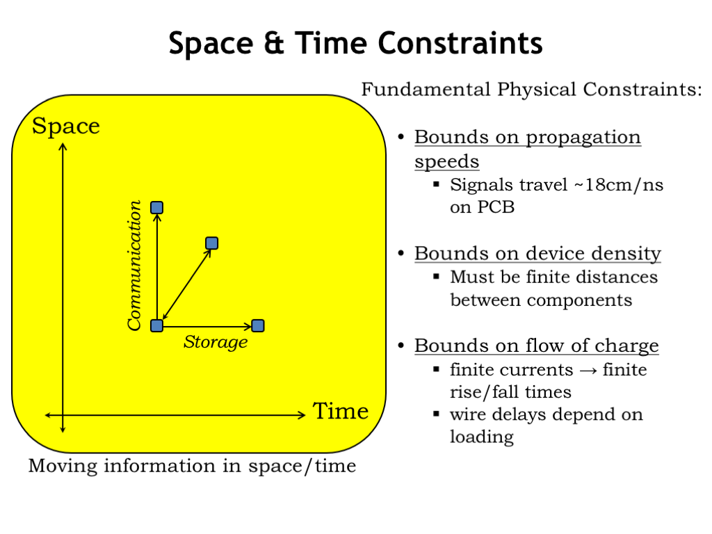
Okay, enough electrical engineering! Suppose we have some information in our system. If we preserve that information over time, we call that storage. If we send that information to another component, we call that communication. In the real world, we’ve seen that communication takes time and we have to budget for that time in our system timing. Our engineering has to accommodate the fundamental bounds on propagating speeds, distances between components and how fast we can change wire voltages without triggering the effects we saw on the previous slide. The upshot: our timing models will have to account for wire delays.
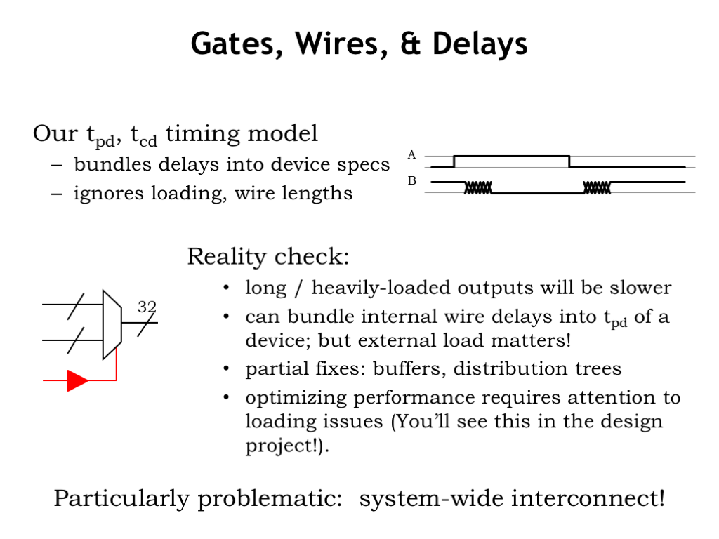
Earlier in the course, we had a simple timing model that assigned a fixed propagation delay, \(t_{\textrm{PD}}\), to the time it took for the output of a logic gate to reflect a change to the gate’s input.
We’ll need to change our timing model to account for delay of transmitting the output of a logic gate to the next components. The timing will be load dependent, so signals that connect to the inputs of many other gates will be slower than signals that connect to only one other gate. The Jade simulator takes the loading of a gate’s output signal into account when calculating the effective propagation delay of the gate.
We can improve propagation delays by reducing the number of loads on output signals or by using specially-design gates called buffers (the component shown in red) to drive signals that have very large loads. A common task when optimizing the performance of a circuit is to track down heavily loaded and hence slow wires and re-engineering the circuit to make them faster.
Today our concern is wires used to connect components at the system level. So next we’ll turn our attention to possible designs for system-level interconnect and the issues that might arise.
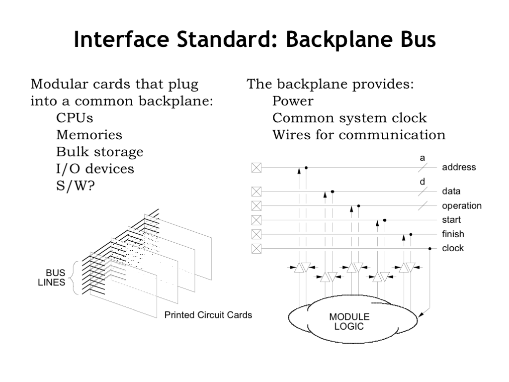
If we want our system to be modular and expandable, how should its design accommodate components that the user might add at a later time? For many years the approach was to provide a way to plug additional printed circuit boards into the main “motherboard” that holds the CPU, memory, and the initial collection of I/O components. The socket on the motherboard connects the circuitry on the add-in card to the signals on the motherboard that allow the CPU to communicate with the add-in card. These signals include power and a clock signal used to time the communication, along with the following.
* Address wires to select different communication end points on the add-in card. The end points might include memory locations, control registers, diagnostic ports, etc.
* Data wires for transferring data to and from the CPU. In older systems, there would many data wires to support byte- or word-width data transfers.
* Some number of control wires that tell the add-in card when a particular transfer has started and that allow the add-in card to indicate when it has responded.
If there are multiple slots for plugging in multiple add-in cards, the same signals might be connected to all the cards and the address wires would be used to sort out which transfers were intended for which cards. Collectively these signals are referred to as the system bus. “Bus” is system architect jargon for a collection of wires used to transfer data using a pre-determined communication protocol.
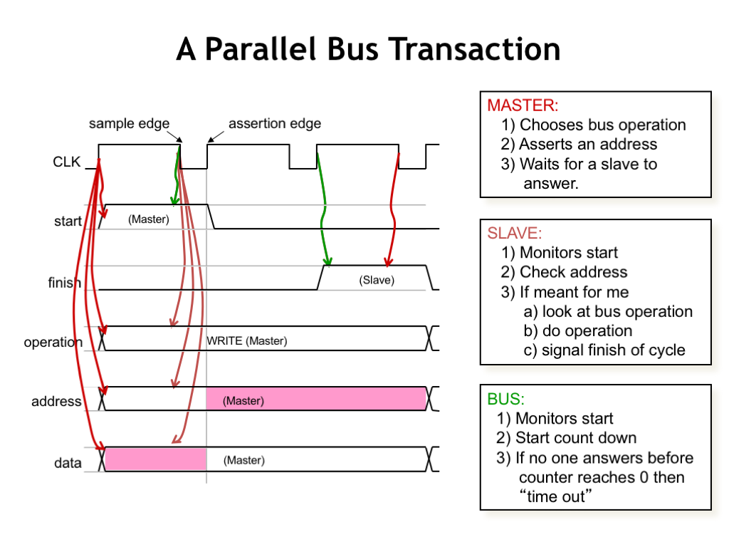
Here’s an example of how a bus transaction might work.
The CLK signal is used to time when signals are placed on the bus wires (at the assertion edge of CLK) and when they’re read by the recipient (at the sample edge of the CLK). The timing of the clock waveform is designed to allow enough time for the signals to propagate down the bus and reach valid logic levels at all the receivers.
The component initiating the transaction is called the bus master who is said to “own” the bus. Most buses provide a mechanism for transferring ownership from one component to another. The master sets the bus lines to indicate the desired operation (read, write, block transfer, etc.), the address of the recipient, and, in the case of a write operation, the data to be sent to the recipient.
The intended recipient, called the slave, is watching the bus lines looking for its address at each sample edge. When it sees a transaction for itself, the slave performs the requested operation, using a bus signal to indicate when the operation is complete. On completion it may use the data wires to return information to the master.
The bus itself may include circuitry to look for transactions where the slave isn’t responding and, after an appropriate interval, generate an error response so the master can take the appropriate action.
This sort of bus architecture proved to be a very workable design for accommodating add-in cards as long as the rate of transactions wasn’t too fast, say less than 50 MHz.

But as system speeds increased, transaction rates had to increase to keep system performance at acceptable levels, so the time for each transaction got smaller. With less time for signaling on the bus wires, various effects began loom large.
If the clock had too short a period, there wasn’t enough time for the master to see the assertion edge, enable its drivers, have the signal propagate down a long bus to the intended receiver and be stable at each receiver for long enough before the sample edge.
Another problem was that the clock signal would arrive at different cards at different times. So a card with an early-arriving clock might decide it was its turn to start driving the bus signals, while a card with a late-arriving clock might still be driving the bus from the previous cycle. These momentary conflicts between drivers could add huge amounts of electrical noise to the system.
Another big issue is that energy would reflect off all the small impedance discontinuities caused by the bus connectors. If there were many connectors, there would be many small echoes which could corrupt the signal seen by various receivers. The equations in the upper right show how much of the signal energy is transmitted and how much is reflected at each discontinuity. The net effect was like trying to talk very fast while yelling into the Grand Canyon — the echoes could distort the message beyond recognition unless sufficient time was allocated between words for the echoes to die away.
Eventually buses were relegated to relatively low-speed communication tasks and a different approach had to be developed for high-speed communication.
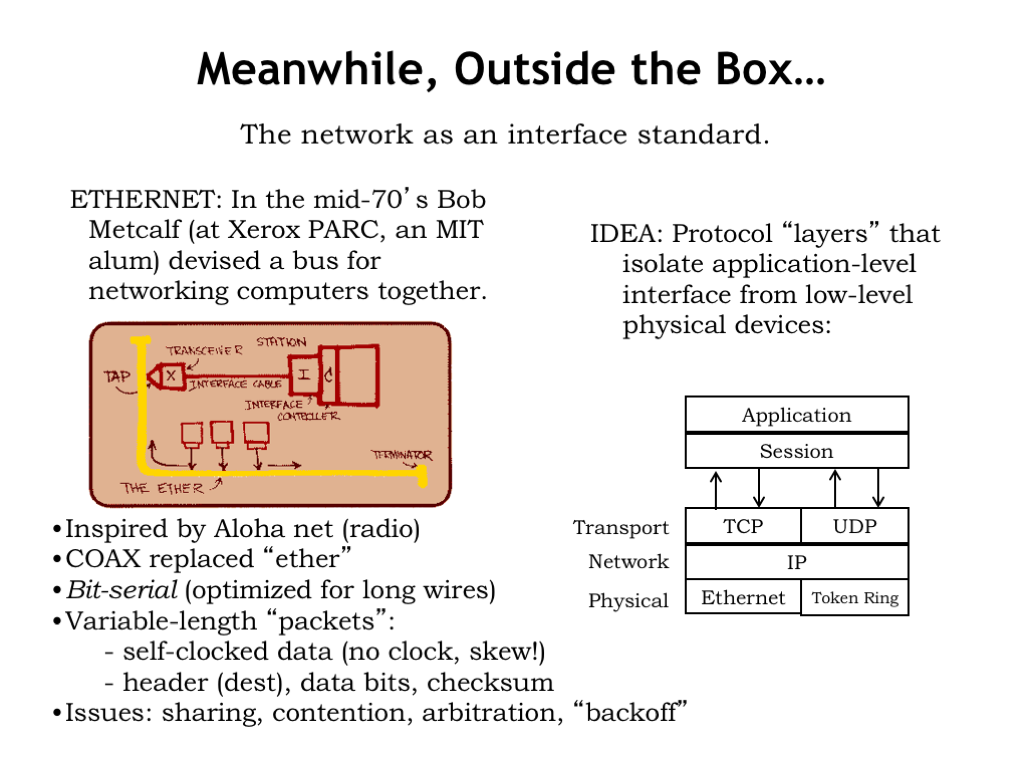
Network technologies were developed to connect components (in this case individual computer systems) separated by larger distances, i.e., distances measured in meters instead of centimeters. Communicating over these larger distances led to different design tradeoffs. In early networks, information was sent as a sequence of bits over the shared communication medium. The bits were organized into packets, each containing the address of the destination. Packets also included a checksum used to detect errors in transmission and the protocol supported the ability to request the retransmission of corrupted packets.
The software controlling the network is divided into a “stack” of modules, each implementing a different communication abstraction. The lowest-level physical layer is responsible for transmitting and receiving an individual packet of bits. Bit errors are detected and corrected, and packets with uncorrectable errors are discarded. There are different physical-layer modules available for the different types of physical networks.
The network layer deals with the addressing and routing of packets. Clever routing algorithms find the shortest communication path through the multi-hop network and deal with momentary or long-term outages on particular network links.
The transport layer is responsible for providing the reliable communication of a stream of data, dealing with the issues of discarded or out-of-order packets. In an effort to optimize network usage and limit packet loses due to network congestion, the transport layer deals with flow control, i.e., the rate at which packets are sent.
A key idea in the networking community is the notion of building a reliable communication channel on top of a “best efforts” packet network. Higher layers of the protocol are designed so that its possible to recover from errors in the lower layers. This has proven much more cost-effective and robust than trying to achieve 100% reliability at each layer.
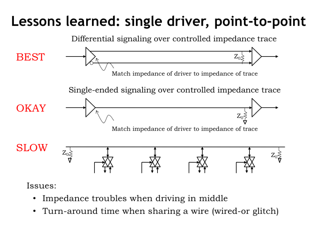
As we saw in the previous section, there are a lot of electrical issues when trying to communicate over a shared wire with multiple drivers and receivers. Slowing down the rate of communication helps to solve the problems, but “slow” isn’t in the cards for today’s high-performance systems.
Experience in the network world has shown that the fastest and least problematic communication channels have a single driver communicating with a single receiver, what’s called a point-to-point link. Using differential signaling is particularly robust. With differential signaling, the receiver measures the voltage difference across the two signaling wires. Electrical effects that might induce voltage noise on one signaling wire will affect the other in equal measure, so the voltage difference will be largely unaffected by most noise. Almost all high-performance communication links use differential signaling.
If we’re sending digital data, does that mean we also have to send a separate clock signal so the receiver knows when to sample the signal to determine the next bit?
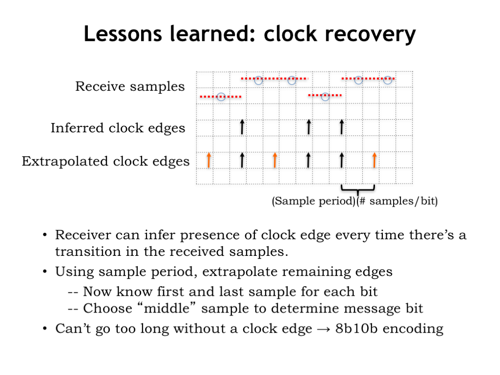
With some cleverness, it turns out that we can recover the timing information from the received signal assuming we know the nominal clock period at the transmitter. If the transmitter changes the bit its sending at the rising edge of the transmitter’s clock, then the receiver can use the transitions in the received waveform to infer the timing for some of the clock edges.
Then the receiver can use its knowledge of the transmitter’s nominal clock period to infer the location of the remaining clock edges. It does this by using a phase-locked loop to generate a local facsimile of the transmitter’s clock, using any received transitions to correct the phase and period of the local clock. The transmitter adds a training sequence of bits at the front of packet to ensure that the receiver’s phased-lock loop is properly synchronized before the packet data itself is transmitted. A special unique bit sequence is used to separate the training signal from the packet data so the receiver can tell exactly where the packet data starts even if it missed a few training bits while the clocks were being properly synchronized.
Once the receiver knows the timing of the clock edges, it can then sample the incoming waveform towards the end of each clock period to determine the transmitted bit.
To keep the local clock in sync with the transmitter’s clock, the incoming waveform needs to have reasonably frequent transitions. But if the transmitter is sending say, all zeroes, how can we guarantee frequent-enough clock edges?
The trick, invented by IBM, is for the transmitter to take the stream of message bits and re-encode them into a bit stream that is guaranteed to have transitions no matter what the message bits are. The most commonly used encoding is 8b10b, where 8 message bits are encoded into 10 transmitted bits, where the encoding guarantees a transition at least every 6 bit times. Of course, the receiver has to reverse the 8b10b encoding to recover the actual message bits. Pretty neat!
The benefit of this trick is that we truly only need to send a single stream of bits. The receiver will be able to recover both the timing information and the data without also needing to transmit a separate clock signal.
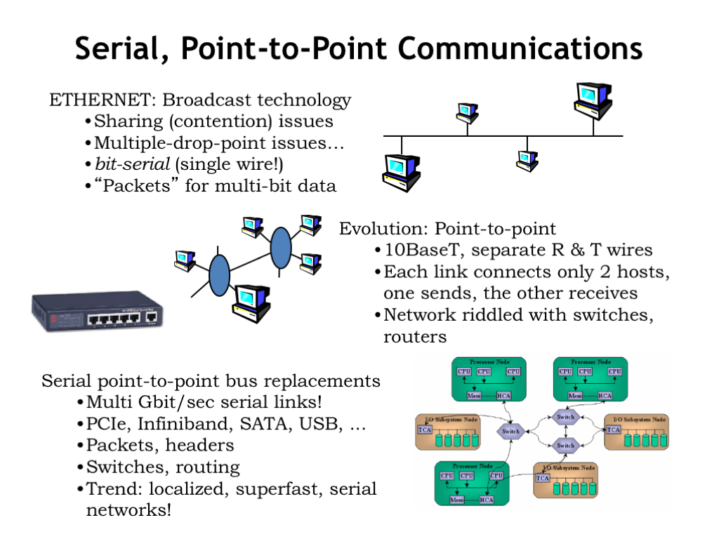
Using these lessons, networks have evolved from using shared communication channels to using point-to-point links. Today local-area networks use 10, 100, or 1000 BaseT wiring which includes separate differential pairs for sending and receiving, i.e., each sending or receiving channel is unidirectional with a single driver and single receiver. The network uses separate switches and routers to receive packets from a sender and then forward the packets over a point-to-point link to the next switch, and so on, across multiple point-to-point links until the packet arrives at its destination.
System-level connections have evolved to use the same communication strategy: point-to-point links with switches for routing packets to their intended destination. Note that communication along each link is independent, so a network with many links can actually support a lot of communication bandwidth. With a small amount of packet buffering in the switches to deal with momentary contention for a particular link, this is a very effective strategy for moving massive amounts of information from one component to the next.
In the next section, we’ll look at some of the more interesting details.
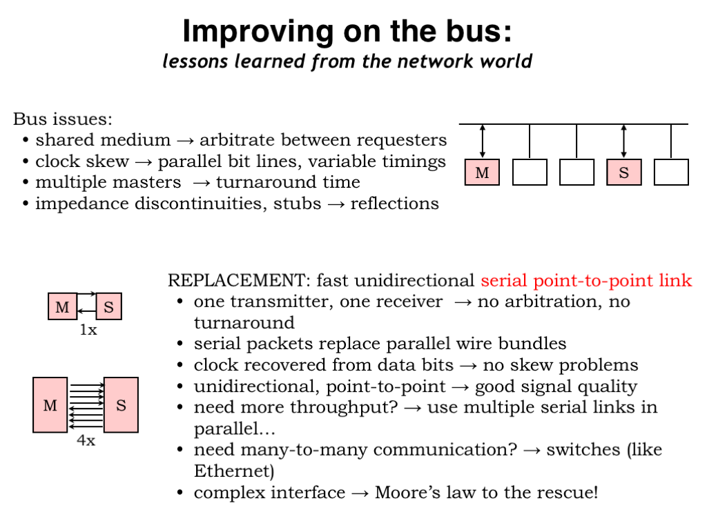
Serial point-to-point links are the modern replacement for the parallel communications bus with all its electrical and timing issues. Each link is unidirectional and has only a single driver and the receiver recovers the clock signal from the data stream, so there are no complications from sharing the channel, clock skew, and electrical problems. The very controlled electrical environment enables very high signaling rates, well up into the gigahertz range using today’s technologies.
If more throughput is needed, you can use multiple serial links in parallel. Extra logic is needed to reassemble the original data from multiple packets sent in parallel over multiple links, but the cost of the required logic gates is very modest in current technologies.
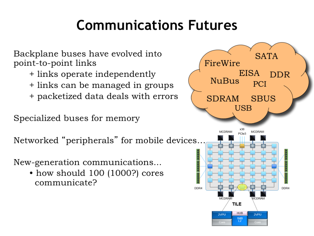
Note that the expansion strategy of modern systems still uses the notion of an add-in card that plugs into the motherboard. But instead of connecting to a parallel bus, the add-in card connects to one or more point-to-point communication links.
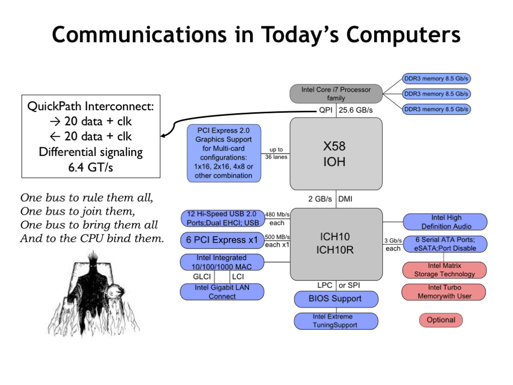
Here’s the system-level communications diagram for a recent system based on an Intel Core i7 CPU chip. The CPU is connected directly to the memories for the highest-possible memory bandwidth, but talks to all the other components over the QuickPath Interconnect (QPI), which has 20 differential signaling paths in each direction. QPI supports up to 6.4 billion 20-bit transfers in each direction every second.
All the other communication channels (USB, PCIe, networks, Serial ATA, Audio, etc.) are also serial links, providing various communication bandwidths depending on the application.
Reading about the QPI channel used by the CPU reminded me a lot of the one ring that could be used to control all of Middle Earth in the Tolkien trilogy Lord of the Rings. Why mess around with a lot of specialized communication channels when you have a single solution that’s powerful enough to solve all your communication needs?

PCI Express (PCIe) is often used as the communication link between components on the system motherboard. A single PCIe version 2 “lane” transmits data at 5 Gb/sec using low-voltage differential signal (LVDS) over wires designed to have a 100-Ohm characteristic impedance.
The PCIe lane is under the control of the same sort of network stack as described earlier. The physical layer transmits packetized data through the lane. Each packet starts with a training sequence to synchronize the receiver’s clock-recovery circuitry, followed by a unique start sequence, then the packet’s data payload, and ends with a unique end sequence.
The physical layer payload is organized as a sequence number, a transaction layer payload and a cyclical redundancy check sequence that’s used to validate the data. Using the sequence number, the data link layer can tell when a packet has been dropped and request the transmitter restart transmission at the missing packet. It also deals with flow control issues.
Finally, the transaction layer reassembles the message from the transaction layer payloads from all the lanes and uses the header to identify the intended recipient at the receive end.
Altogether, a significant amount of logic is needed to send and receive messages on multiple PCIe lanes, but the cost is quite acceptable when using today’s integrated circuit technologies. Using 8 lanes, the maximum transfer rate is 4 GB/sec, capable of satisfying the needs of high-performance peripherals such as graphics cards.
So knowledge from the networking world has reshaped how components communicate on the motherboard, driving the transition from parallel buses to a handful of serial point-to-point links. As a result today’s systems are faster, more reliable, more energy-efficient and smaller than ever before.

Let’s wrap up our discussion of system-level interconnect by considering how best to connect N components that need to send messages to one another, e.g., CPUs on a multicore chip. Today such chips have a handful of cores, but soon they may have 100s or 1000s of cores.
We’ll build our communications network using point-to-point links. In our analysis, each point-to-point link is counted at a cost of 1 hardware unit. Sending a message across a link requires one time unit. And we’ll assume that different links can operate in parallel, so more links will mean more message traffic.
We’ll do an asymptotic analysis of the throughput (total messages per unit time), latency (worst-case time to deliver a single message), and hardware cost. In other words, we’ll make a rough estimate how these quantities change as N grows.
Note that in general the throughput and hardware cost are proportional to the number of point-to-point links.
Our baseline is the backplane bus discussed earlier, where all the components share a single communication channel. With only a single channel, bus throughput is 1 message per unit time and a message can travel between any two components in one time unit. Since each component has to have an interface to the shared channel, the total hardware cost is O(n).
In a ring network each component sends its messages to a single neighbor and the links are arranged so that its possible to reach all components. There are N links in total, so the throughput and cost are both O(n). The worst case latency is also O(n) since a message might have to travel across N-1 links to reach the neighbor that’s immediately upstream. Ring topologies are useful when message latency isn’t important or when most messages are to the component that’s immediately downstream, i.e., the components form a processing pipeline.

The most general network topology is when every component has a direct link to every other component. There are O(N**2) links so the throughput and cost are both O(N**2). And the latency is 1 time unit since each destination is directly accessible. Although expensive, complete graphs offer very high throughput with very low latencies.
A variant of the complete graph is the crossbar switch where a particular row and column can be connected to form a link between particular A and B components with the restriction that each row and each column can only carry 1 message during each time unit. Assume that the first row and first column connect to the same component, and so on, i.e., that the example crossbar switch is being used to connect 4 components. Then there are O(n) messages delivered each time unit, with a latency of 1. There are N**2 switches in the crossbar, so the cost is O(N**2) even though there are only O(n) links.
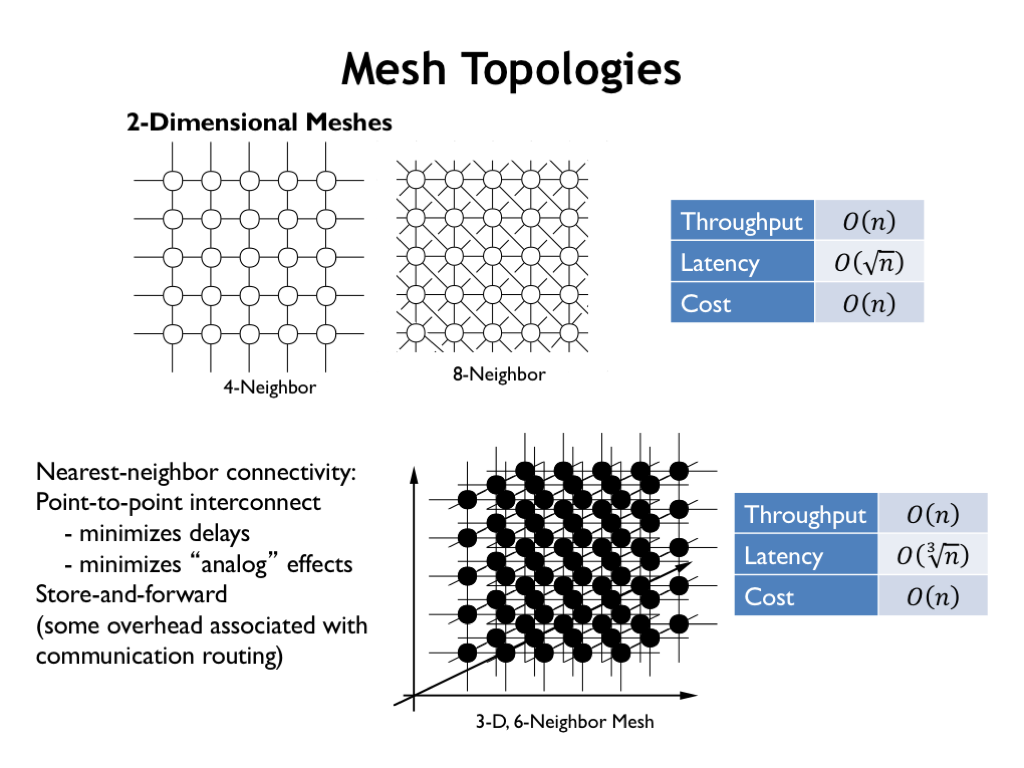
In mesh networks, components are connected to some fixed number of neighboring components, in either 2- or 3-dimensions. Hence the total number of links is proportional to the number of components, so both throughput and cost are O(n). The worst-case latencies for mesh networks are proportional to length of the sides, so the latency is O(sqrt n) for 2D meshes and O(cube root n) for 3D meshes. The orderly layout, constant per-node hardware costs, and modest worst-case latency make 2D 4-neighbor meshes a popular choice for the current generation of experimental multi-core processors.
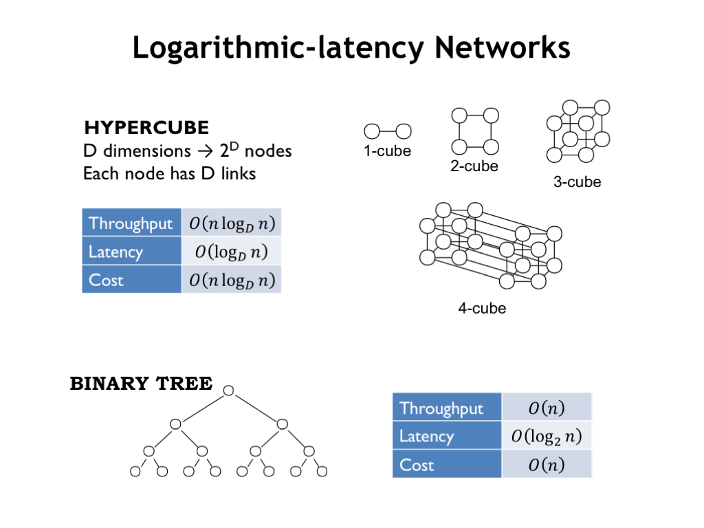
Hypercube and tree networks offer logarithmic latencies, which for large N may be faster than mesh networks. The original CM-1 Connection Machine designed in the 80’s used a hypercube network to connect up to 65,536 very simple processors, each connected to 16 neighbors. Later generations incorporated smaller numbers of more sophisticated processors, still connected by a hypercube network. In the early 90’s the last generation of Connection Machines used a tree network, with the clever innovation that the links towards the root of the tree had a higher message capacity.
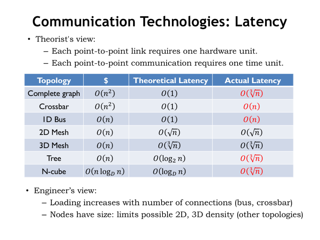
Here’s a summary of the theoretical latencies we calculated for the various topologies.
As a reality check, it’s important to realize that the lower bound on the worst-case distance between components in our 3-dimensional world is O(cube root of N). In the case of a 2D layout, the worst-case distance is O(sqrt N). Since we know that the time to transmit a message is proportional to the distance traveled, we should modify our latency calculations to reflect this physical constraint.
Note that the bus and crossbar involve N connections to a single link, so here the lower-bound on the latency needs to reflect the capacitive load added by each connection.
The winner? Mesh networks avoid the need for longer wires as the number of connected components grows and appear to be an attractive alternative for high-capacity communication networks connecting 1000’s of processors.
Summarizing our discussion:
- Point-to-point links are in common use today for system-level interconnect, and as a result our systems are faster, more reliable, more energy-efficient and smaller than ever before.
- Multi-signal parallel buses are still used for very-high-bandwidth connections to memories, with a lot of very careful engineering to avoid the electrical problems observed in earlier bus implementations.
- Wireless connections are in common use to connect mobile devices to nearby components and there has been interesting work on how to allow mobile devices to discover what peripherals are nearby and enable them to connect automatically.
- The upcoming generation of multi-core chips will have 10’s to 100’s of processing cores. There is a lot ongoing research to determine which communication topology would offer the best combination of high communication bandwidth and low latency. The next ten years will be an interesting time for on-chip network engineers!
- BackSystem-level Communication
- ContinueTopic Videos


