
L04: Combinational Logic
- Functional Specifications
- Here’s a Design Approach
- Sum-of-products Building Blocks
- Straightforward Synthesis
- ANDs and ORs with > 2 Inputs
- More Building Blocks
- Universal Building Blocks
- CMOS Loves Inverting Logic
- Wide NANDs and NORs
- CMOS Sum-of-products Implementation
- Logic Simplification
- Boolean Minimization
- Truth Tables with Don’t Cares
- The Case for a Non-minimal SOP
- Karnuagh Maps: A Geometric Approach
- Extending K-maps to 4-variable Tables
- Finding Implicants
- Finding Prime Implicants
- Write Down Equations
- Prime Implicants, Glitches & Leniency
- We’ve Been Designing a MUX
- Systematic Implementation Strategies
- Synthesis By Table Lookup
- Read-only Memory (ROM)
- ROM Example
- ROM Example continued
- Faster ROMs
- Logic According to ROMs
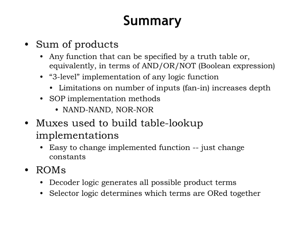
- Summary
Content of the following slides is described in the surrounding text.
In this lecture, you’ll learn various techniques for creating combinational logic circuits that implement a particular functional specification.
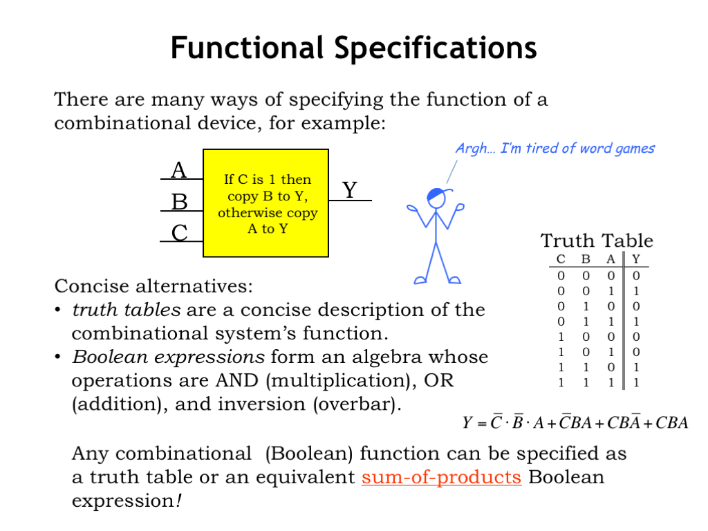
A functional specification is part of the static discipline we use to build the combinational logic abstraction of a circuit. One approach is to use natural language to describe the operation of a device. This approach has its pros and cons. In its favor, natural language can convey complicated concepts in surprisingly compact form and it is a notation that most of us know how to read and understand. But, unless the words are very carefully crafted, there may be ambiguities introduced by words with multiple interpretations or by lack of completeness since it’s not always obvious whether all eventualities have been dealt with.
There are good alternatives that address the shortcomings mentioned above. Truth tables are a straightforward tabular representation that specifies the values of the outputs for each possible combination of the digital inputs. If a device has N digital inputs, its truth table will have \(2^N\) rows. In the example shown here, the device has 3 inputs, each of which can have the value 0 or the value 1. There are \(2 \cdot 2 \cdot 2 = 2^3 = 8\) combinations of the three input values, so there are 8 rows in the truth table. It’s straightforward to systematically enumerate the 8 combinations, which makes it easy to ensure that no combination is omitted when building the specification. And since the output values are specified explicitly, there isn’t much room for misinterpreting the desired functionality!
Truth tables are an excellent choice for devices with small numbers of inputs and outputs. Sadly, they aren’t really practical when the devices have many inputs. If, for example, we were describing the functionality of a circuit to add two 32-bit numbers, there would be 64 inputs altogether and the truth table would need \(2^{64}\) rows. Hmm, not sure how practical that is! If we entered the correct output value for a row once per second, it would take 584 billion years to fill in the table!
Another alternative specification is to use Boolean equations to describe how to compute the output values from the input values using Boolean algebra. The operations we use are the logical operations AND, OR, and XOR, each of which takes two Boolean operands, and NOT which takes a single Boolean operand. Using the truth tables that describe these logical operations, it’s straightforward to compute an output value from a particular combination of input values using the sequence of operations laid out in the equation.
Let me say a quick word about the notation used for Boolean equations. Input values are represented by the name of the input, in this example one of A, B, or C. The digital input value 0 is equivalent to the Boolean value FALSE and the digital input value 1 is equivalent to the Boolean value TRUE.
The Boolean operation NOT is indicated by a horizontal line drawn above a Boolean expression. In this example, the first symbol following the equal sign is a C with line above it, indicating that the value of C should be inverted before it’s used in evaluating the rest of the expression.
The Boolean operation AND is represented by the multiplication operation using standard mathematical notation. Sometimes we’ll use an explicit multiplication operator — usually written as a dot between two Boolean expressions — as shown in the first term of the example equation. Sometimes the AND operator is implicit as shown in the remaining three terms of the example equation.
The Boolean operation OR is represented by the addition operation, always shown as a “+” sign.
Boolean equations are useful when the device has many inputs. And, as we’ll see, it’s easy to convert a Boolean equation into a circuit schematic.
Truth tables and Boolean equations are interchangeable. If we have a Boolean equation for each output, we can fill in the output columns for a row of the truth table by evaluating the Boolean equations using the particular combination of input values for that row. For example, to determine the value for Y in the first row of the truth table, we’d substitute the Boolean value FALSE for the symbols A, B, and C in the equation and then use Boolean algebra to compute the result.
We can go the other way too. We can always convert a truth table into a particular form of Boolean equation called a sum-of-products. Let’s see how…
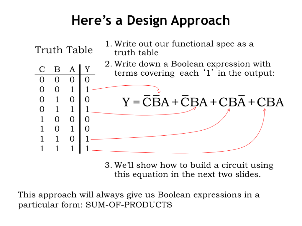
Start by looking at the truth table and answering the question “When does Y have the value 1?” Or in the language of Boolean algebra: “When is Y TRUE?” Well, Y is TRUE when the inputs correspond to row 2 of the truth table, OR to row 4, OR to rows 7 OR 8. Altogether there are 4 combinations of inputs for which Y is TRUE. The corresponding Boolean equation thus is the OR for four terms, where each term is a Boolean expression which evaluates to TRUE for a particular combination of inputs.
Row 2 of the truth table corresponds to C=0, B=0, and A=1. The corresponding Boolean expression is \(\overline{C} \cdot \overline{B} \cdot A\), an expression that evaluates to TRUE if and only if C is 0, B is 0, and A is 1.
The Boolean expression corresponding to row 4 is \(\overline{C} \cdot B \cdot A\). And so on for rows 7 and 8.
This approach will always give us an expression in the form of a sum-of-products. “Sum” refers to the OR operations and “products” refers to the groups of AND operations. In this example, we have the sum of four product terms.
Our next step is to use the Boolean expression as a recipe for constructing a circuit implementation using combinational logic gates.
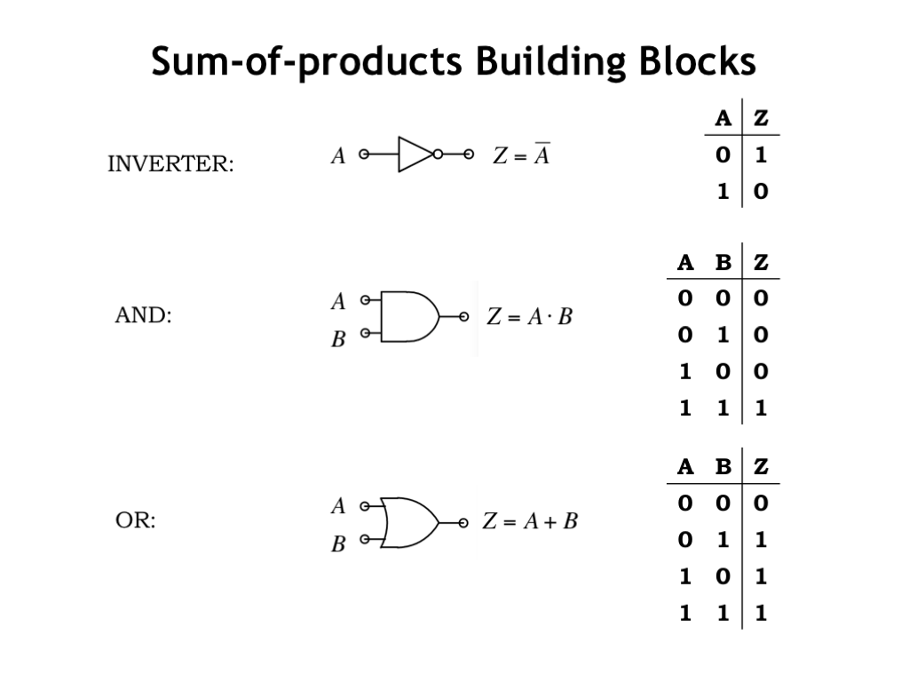
As circuit designers, we’ll be working with a library of combinational logic gates, which either is given to us by the integrated circuit manufacturer, or which we’ve designed ourselves as CMOS gates using NFET and PFET switches.
One of the simplest gates is the inverter, which has the schematic symbol shown here. The small circle on the output wire indicates an inversion, a common convention used in schematics. We can see from its truth table that the inverter implements the Boolean NOT function.
The AND gate outputs 1 if and only if the A input is 1 and the B input is 1, hence the name AND. The library will usually include AND gates with 3 inputs, 4 inputs, etc., which produce a 1 output if and only if all of their inputs are 1.
The OR gate outputs 1 if the A input is 1 *or* if the B input is 1, hence the name OR. Again, the library will usually include OR gates with 3 inputs, 4 inputs, etc., which produce a 1 output when at least one of their inputs is 1.
These are the standard schematic symbols for AND and OR gates. Note that the AND symbol is straight on the input side, while the OR symbol is curved. With a little practice, you’ll find it easy to remember which schematic symbols are which.
Now let’s use these building blocks to build a circuit that implements a sum-of-products Boolean equation.
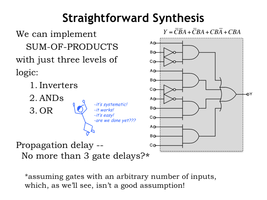
The structure of the circuit exactly follows the structure of the Boolean equation. We use inverters to perform the necessary Boolean NOT operations. In a sum-of-products equation the inverters are operating on particular input values, in this case A, B and C. To keep the schematic easy to read we’ve used a separate inverter for each of the four NOT operations in the Boolean equation, but in real life we might invert the C input once to produce a NOT-C signal, then use that signal whenever a NOT-C value is needed.
Each of the four product terms is built using a 3-input AND gate. And the product terms are ORed together using a 4-input OR gate. The final circuit has a layer of inverters, a layer of AND gates and final OR gate. In the next section, we’ll talk about how to build AND or OR gates with many inputs from library components with fewer inputs.
The propagation delay for a sum-of-products circuit looks pretty short: the longest path from inputs to outputs includes an inverter, an AND gate and an OR gate. Can we really implement any Boolean equation in a circuit with a \(t_{\textrm{PD}}\) of three gate delays?
Actually not, since building ANDs and ORs with many inputs will require additional layers of components, which will increase the propagation delay. We’ll learn about this in the next section.
The good news is that we now have straightforward techniques for converting a truth table to its corresponding sum-of-products Boolean equation, and for building a circuit that implements that equation.
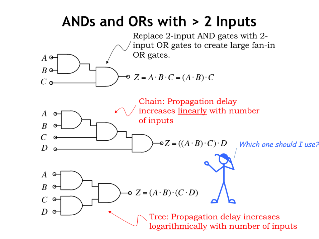
On our to-do list from the previous section is figuring out how to build AND and OR gates with many inputs. These will be needed when creating circuit implementations using a sum-of-products equation as our template. Let’s assume our gate library only has 2-input gates and figure how to build wider gates using the 2-input gates as building blocks. We’ll work on creating 3- and 4-input gates, but the approach we use can be generalized to create AND and OR gates of any desired width.
The approach shown here relies on the associative property of the AND operator. This means we can perform an N-way AND by doing pair-wise ANDs in any convenient order. The OR and XOR operations are also associative, so the same approach will work for designing wide OR and XOR circuits from the corresponding 2-input gate. Simply substitute 2-input OR gates or 2-input XOR gates for the 2-input AND gates shown below and you’re good to go!
Let’s start by designing a circuit that computes the AND of three inputs A, B, and C. In the circuit shown here, we first compute (A AND B), then AND that result with C.
Using the same strategy, we can build a 4-input AND gate from three 2-input AND gates. Essentially we’re building a chain of AND gates, which implement an N-way AND using N-1 2-input AND gates.
We can also associate the four inputs a different way: computing (A AND B) in parallel with (C AND D), then combining those two results using a third AND gate. Using this approach, we’re building a tree of AND gates.
Which approach is best: chains or trees? First we have to decide what we mean by “best.” When designing circuits, we’re interested in cost, which depends on the number of components, and performance, which we characterize by the propagation delay of the circuit.
Both strategies require the same number of components since the total number of pair-wise ANDs is the same in both cases. So it’s a tie when considering costs. Now consider propagation delay.
The chain circuit in the middle has a \(t_{\textrm{PD}}\) of 3 gate delays, and we can see that the \(t_{\textrm{PD}}\) for an N-input chain will be N-1 gate delays. The propagation delay of chains grows linearly with the number of inputs.
The tree circuit on the bottom has a \(t_{\textrm{PD}}\) of 2 gates, smaller than the chain. The propagation delay of trees grows logarithmically with the number of inputs. Specifically, the propagation delay of tree circuits built using 2-input gates grows as log2(N). When N is large, tree circuits can have dramatically better propagation delay than chain circuits.
The propagation delay is an upper bound on the worst-case delay from inputs to outputs and is a good measure of performance assuming that all inputs arrive at the same time. But in large circuits, A, B, C and D might arrive at different times depending on the \(t_{\textrm{PD}}\) of the circuit generating each one. Suppose input D arrives considerably after the other inputs. If we used the tree circuit to compute the AND of all four inputs, the additional delay in computing Z is two gate delays after the arrival of D. However, if we use the chain circuit, the additional delay in computing Z might be as little as one gate delay.
The moral of this story: it’s hard to know which implementation of a subcircuit, like the 4-input AND shown here, will yield the smallest overall \(t_{\textrm{PD}}\) unless we know the \(t_{\textrm{PD}}\) of the circuits that compute the values for the input signals.
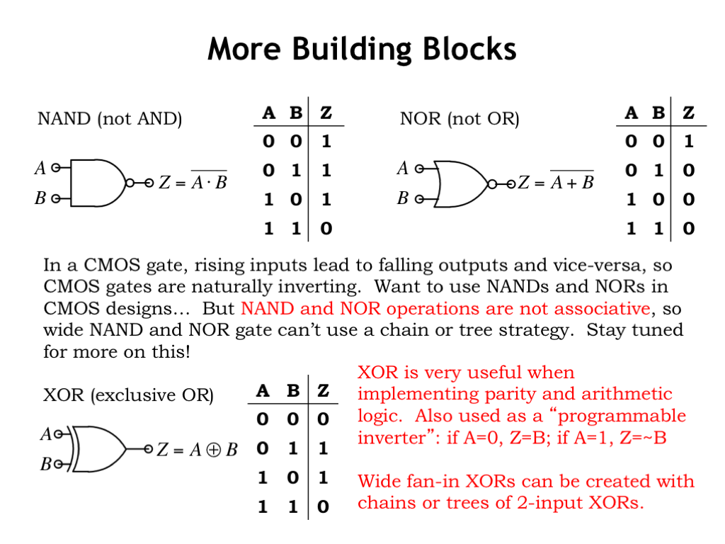
In designing CMOS circuits, the individual gates are naturally inverting, so instead of using AND and OR gates, for the best performance we want to the use the NAND and NOR gates shown here. NAND and NOR gates can be implemented as a single CMOS gate involving one pullup circuit and one pulldown circuit. AND and OR gates require two CMOS gates in their implementation, e.g., a NAND gate followed by an INVERTER. We’ll talk about how to build sum-of-products circuitry using NANDs and NORs in the next section.
Note that NAND and NOR operations are not associative: NAND(A,B,C) is not equal to NAND(NAND(A,B),C). So we can’t build a NAND gate with many inputs by building a tree of 2-input NANDs. We’ll talk about this in the next section too!
We’ve mentioned the exclusive-or operation, sometimes called XOR, several times. This logic function is very useful when building circuitry for arithmetic or parity calculations. As you’ll see in Lab 2, implementing a 2-input XOR gate will take many more NFETs and PFETs than required for a 2-input NAND or NOR.
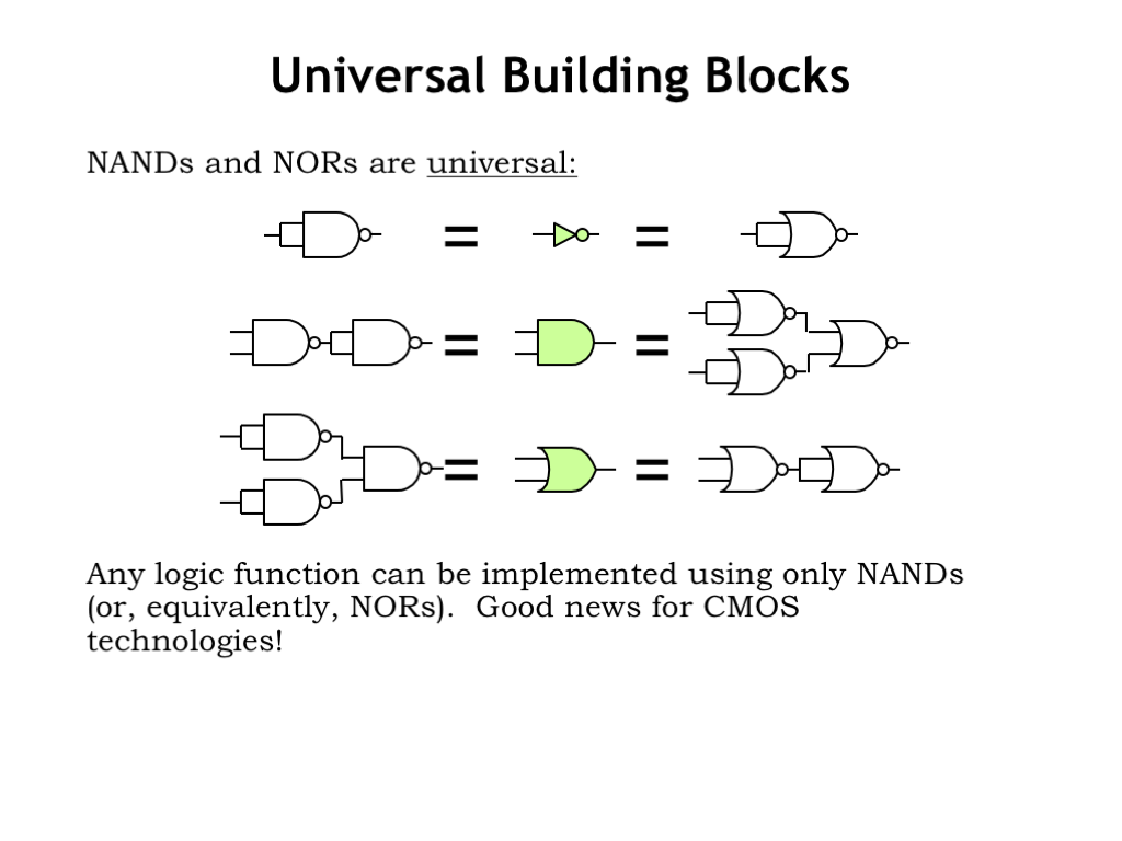
We know we can come up with a sum-of-products expression for any truth table and hence build a circuit implementation using INVERTERs, AND gates, and OR gates. It turns out we can build circuits with the same functionality using only 2-INPUT NAND gates — we say the 2-INPUT NAND is a universal gate.
Here we show how to implement the sum-of-products building blocks using just 2-input NAND gates. In a minute we’ll show a more direct implementation for sum-of-products using only NANDs, but these little schematics are a proof-of-concept showing that NAND-only equivalent circuits exist.
2-INPUT NOR gates are also universal, as shown by these little schematics.
Inverting logic takes a little getting used to, but it’s the key to designing low-cost high-performance circuits in CMOS.
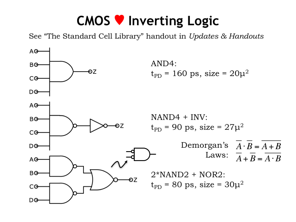
Now would be a good time to take a moment to look at the documentation for the library of logic gates we’ll use for our designs — look for The Standard Cell Library handout. The information on this slide is taken from there.
The library has both inverting gates (such as inverters, NANDs and NORs) and non-inverting gates (such as buffers, ANDs and ORs). Why bother to include both types of gates? Didn’t we just learn we can build any circuit using only NAND or NOR?
Good questions! We get some insight into the answers if we look at these three implementations for a 4-input AND function.
The upper circuit is a direct implementation using the 4-input AND gate available in the library. The \(t_{\textrm{PD}}\) of the gate is 160 picoseconds and its size is 20 square microns. Don’t worry too much about the actual numbers, what matters on this slide is how the numbers compare between designs.
The middle circuit implements the same function, this time using a 4-INPUT NAND gate hooked to an inverter to produce the AND functionality we want. The \(t_{\textrm{PD}}\) of this circuit is 90 picoseconds, considerably faster than the single gate above. The tradeoff is that the size is somewhat larger.
How can this be? Especially since we know the AND gate implementation is the NAND/INVERTER pair shown in the middle circuit. The answer is that the creators of the library decided to make the non-inverting gates small but slow by using MOSFETs with much smaller widths than used in the inverting logic gates, which were designed to be fast.
Why would we ever want to use a slow gate? Remember that the propagation delay of a circuit is set by the longest path in terms of delay from inputs to outputs. In a complex circuit, there are many input/output paths, but it’s only the components on the longest path that need to be fast in order to achieve the best possible overall \(t_{\textrm{PD}}\). The components on the other, shorter paths, can potentially be a bit slower. And the components on short input/output paths can be very slow indeed. So for the portions of the circuit that aren’t speed sensitive, it’s a good tradeoff to use slower but smaller gates. The overall performance isn’t affected, but the total size is improved.
So for faster performance we’ll design with inverting gates, and for smallest size we’ll design with non-inverting gates. The creators of the gate library designed the available gates with this tradeoff in mind.
The 4-input inverting gates are also designed with this tradeoff in mind. For the ultimate in performance, we want to use a tree circuit of 2-input gates, as shown in the lower circuit. This implementation shaves 10 picoseconds off the \(t_{\textrm{PD}}\), while costing us a bit more in size.
Take a closer look at the lower circuit. This tree circuit uses two NAND gates whose outputs are combined with a NOR gate. Does this really compute the AND of A, B, C, and D? Yup, as you can verify by building the truth table for this combinational system using the truth tables for NAND and NOR.
This circuit is a good example of the application of a particular Boolean identity known as Demorgan’s Law. There are two forms of Demorgan’s law, both of which are shown here. The top form is the one we’re interested in for analyzing the lower circuit. It tells us that the NOR of A with B is equivalent to the AND of (NOT A) with (NOT B). So the 2-input NOR gate can be thought of as a 2-input AND gate with inverting inputs. How does this help? We can now see that the lower circuit is actually a tree of AND gates, where the inverting outputs of the first layer match up with the inverting inputs of the second layer.
It’s a little confusing the first time you see it, but with practice you’ll be comfortable using Demorgan’s law when building trees or chains of inverting logic.
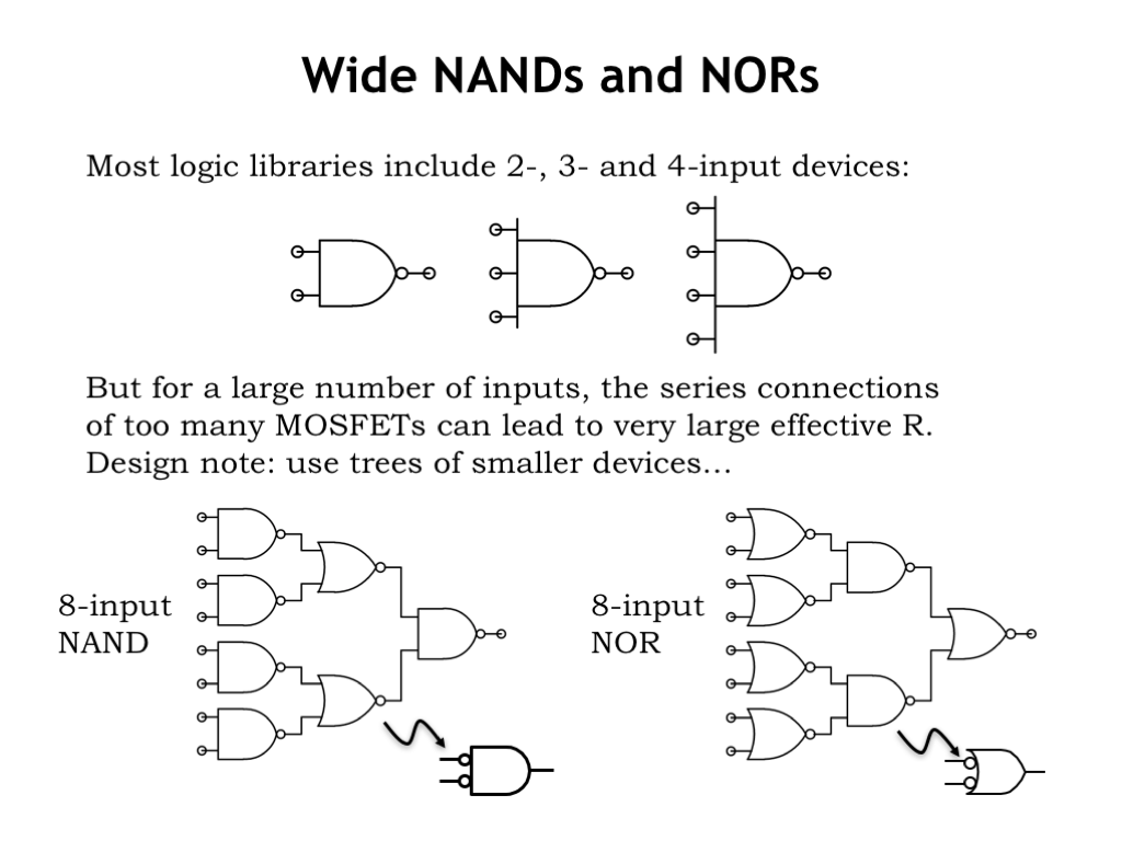
Using Demorgan’s Law we can answer the question of how to build NANDs and NORs with large numbers of inputs. Our gate library includes inverting gates with up to 4 inputs. Why stop there? Well, the pulldown chain of a 4-input NAND gate has 4 NFETs in series and the resistance of the conducting channels is starting to add up. We could make the NFETs wider to compensate, but then the gate gets much larger and the wider NFETs impose a higher capacitive load on the input signals. The number of possible tradeoffs between size and speed grows rapidly with the number of inputs, so it’s usually just best for the library designer to stop at 4-input gates and let the circuit designer take it from there.
Happily, Demorgan’s law shows us how build trees of alternating NANDs and NORs to build inverting logic with a large number of inputs. Here we see schematics for an 8-input NAND and an 8-input NOR gate.
Think of the middle layer of NOR gates in the left circuit as AND gates with inverting inputs and then it’s easy to see that the circuit is a tree of ANDs with an inverting output.
Similarly, think of the middle layer of NAND gates in the right circuit as OR gates with inverting inputs and see that we really have a tree of OR gates with an inverting output.
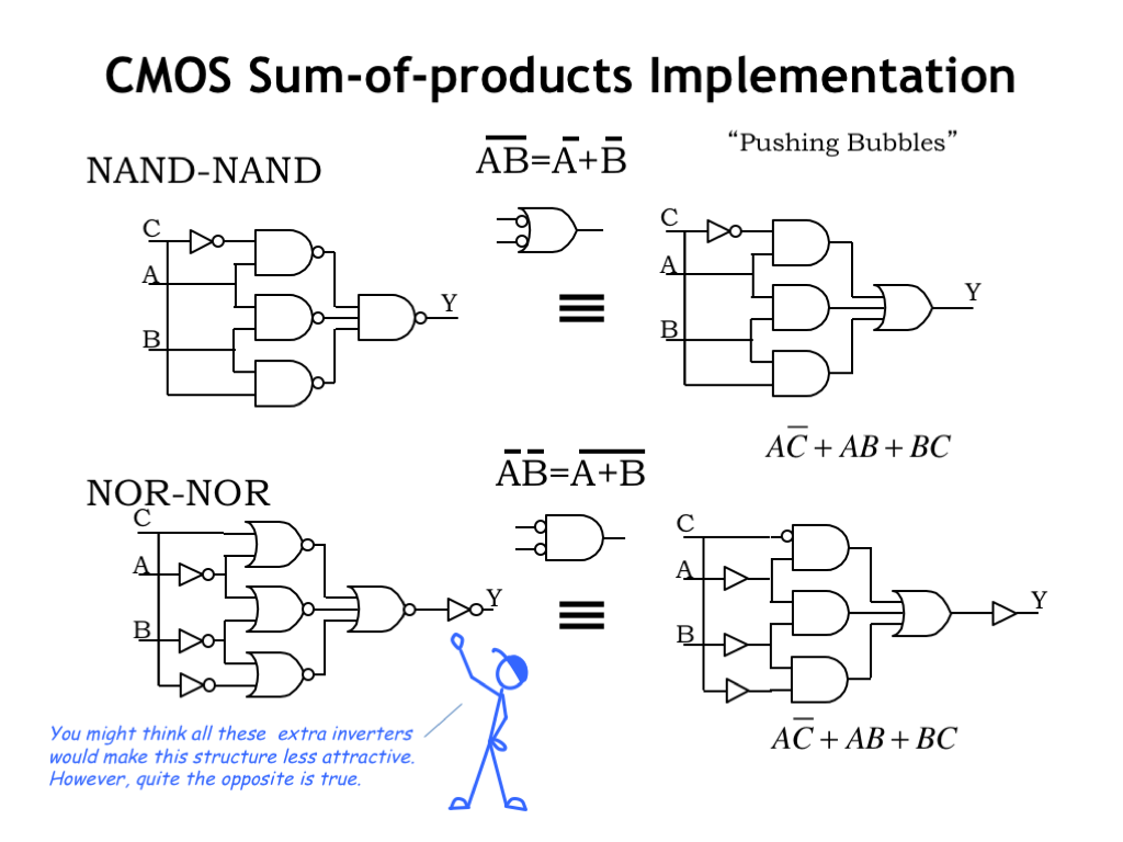
Now let’s see how to build sum-of-products circuits using inverting logic. The two circuits shown here implement the same sum-of-products logic function. The one on the top uses two layers of NAND gates, the one on the bottom, two layers of NOR gates.
Let’s visualize Demorgan’s Law in action on the top circuit. The NAND gate with Y on its output can be transformed by Demorgan’s Law into an OR gate with inverting inputs. So we can redraw the circuit on the top left as the circuit shown on the top right. Now, notice that the inverting outputs of the first layer are cancelled by the inverting inputs of the second layer [CLICK], a step we can show visually by removing matching inversions. And, voila, we see the NAND/NAND circuit in sum-of-products form: a layer of inverters, a layer of AND gates, and an OR gate to combine the product terms.
We can use a similar visualization to transform the output gate of the bottom circuit, giving us the circuit on the bottom right. Match up the bubbles and we see that we have the same logic function as above.
Looking at the NOR/NOR circuit on the bottom left, we see it has 4 inverters, where as the NAND/NAND circuit only has one. Why would we ever use the NOR/NOR implementation? It has to do with the loading on the inputs. In the top circuit, the input A connects to a total of four MOSFET switches. In the bottom circuit, it connects to only the two MOSFET switches in the inverter. So, the bottom circuit imposes half the capacitive load on the A signal. This might be significant if the signal A connected to many such circuits.
The bottom line: when you find yourself needing a fast implementation for the AND/OR circuitry for a sum-of-products expression, try using the NAND/NAND implementation. It’ll be noticeably faster than using AND/OR.
The previous sections showed us how to build a circuit that computes a given sum-of-products expression. An interesting question to ask is if we can implement the same functionality using fewer gates or smaller gates? In other words is there an equivalent Boolean expression that involves fewer operations? Boolean algebra has many identities that can be used to transform an expression into an equivalent, and hopefully smaller, expression.
The reduction identity in particular offers a transformation that simplifies an expression involving two variables and four operations into a single variable and no operations. Let’s see how we might use that identity to simplify a sum-of-products expression.
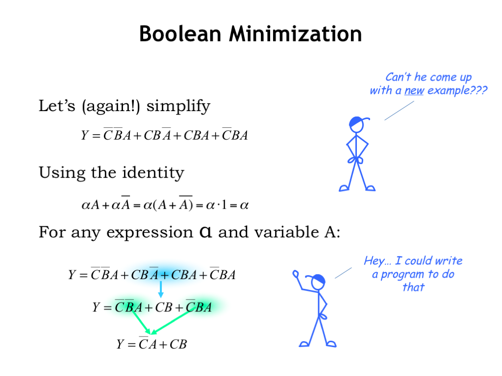
Here’s the equation from the start of this chapter, involving 4 product terms. We’ll use a variant of the reduction identity involving a Boolean expression alpha and a single variable A. Looking at the product terms, the middle two offer an opportunity to apply the reduction identity if we let alpha be the expression (C AND B). So we simplify the middle two product terms to just alpha, i.e., (C AND B), eliminating the variable A from this part of the expression.
Considering the now three product terms, we see that the first and last terms can also be reduced, this time letting alpha be the expression (NOT C and A). Wow, this equivalent equation is much smaller! Counting inversions and pair-wise operations, the original equation has 14 operations, while the simplified equation has 4 operations. The simplified circuit would be much cheaper to build and have a smaller \(t_{\textrm{PD}}\) in the bargain!
Doing this sort of Boolean simplification by hand is tedious and error-prone. Just the sort of task a computer program could help with. Such programs are in common use, but the computation needed to discover the smallest possible form for an expression grows faster than exponentially as the number of inputs increases. So for larger equations, the programs use various heuristics to choose which simplifications to apply. The results are quite good, but not necessarily optimal. But it sure beats doing the simplification by hand!
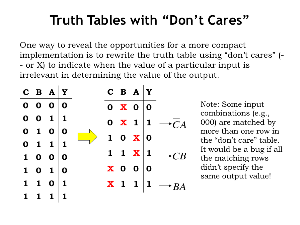
Another way to think about simplification is by searching the truth table for don’t-care situations. For example, look at the first and third rows of the original truth table on the left. In both cases A is 0, C is 0, and the output Y is 0. The only difference is the value of B, which we can then tell is irrelevant when both A and C are 0. This gives us the first row of the truth table on the right, where we use X to indicate that the value of B doesn’t matter when A and C are both 0. By comparing rows with the same value for Y, we can find other don’t-care situations.
The truth table with don’t-cares has only three rows where the output is 1. And, in fact, the last row is redundant in the sense that the input combinations it matches (011 and 111) are covered by the second and fourth rows.
The product terms derived from rows two and four are exactly the product terms we found by applying the reduction identity.
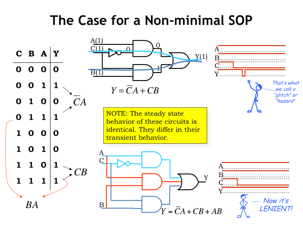
Do we always want to use the simplest possible equation as the template for our circuits? Seems like that would minimize the circuit cost and maximize performance, a good thing.
The simplified circuit is shown here. Let’s look at how it performs when A is 1, B is 1, and C makes a transition from 1 to 0. Before the transition, C is 1 and we can see from the annotated node values that it’s the bottom AND gate that’s causing the Y output to be 1.
When C transitions to 0, the bottom AND gate turns off and the top AND gate turns on, and, eventually the Y output becomes 1 again. But the turning on of the top AND is delayed by the \(t_{\textrm{PD}}\) of the inverter, so there’s a brief period of time where neither AND gate is on, and the output momentarily becomes 0. This short blip in Y’s value is called a glitch and it may result in short-lived changes on many node values as it propagates through other parts of the circuit. All those changes consume power, so it would be good to avoid these sorts of glitches if we can.
If we include the third product term BA in our implementation, the circuit still computes the same long-term answer as before. But now when A and B are both high, the output Y will be 1 independently of the value of the C input. So the 1-to-0 transition on the C input doesn’t cause a glitch on the Y output. If you recall the last section of the previous chapter, the phrase we used to describe such circuits is lenient.
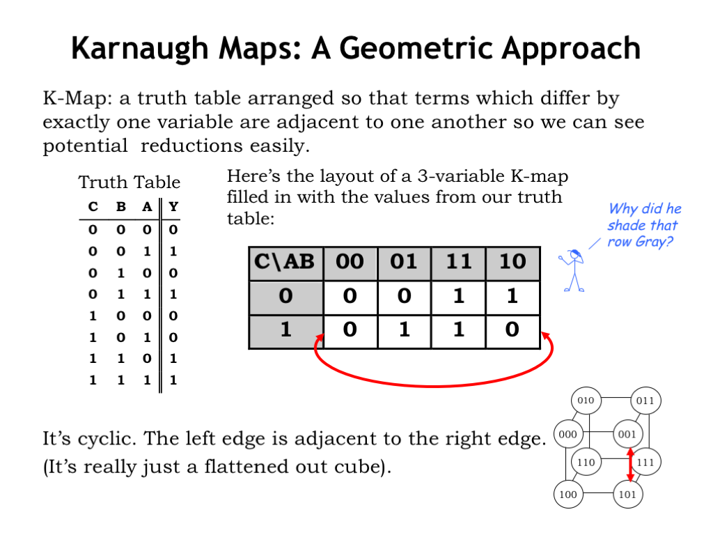
When trying to minimize a sum-of-products expression using the reduction identity, our goal is to find two product terms that can be written as one smaller product term, eliminating the don’t-care variable. This is easy to do when two the product terms come from adjacent rows in the truth table. For example, look at the bottom two rows in this truth table. Since the Y output is 1 in both cases, both rows will be represented in the sum-of-products expression for this function. It’s easy to spot the don’t care variable: when C and B are both 1, the value of A isn’t needed to determine the value of Y. Thus, the last two rows of the truth table can be represented by the single product term (B AND C).
Finding these opportunities would be easier if we reorganized the truth table so that the appropriate product terms were on adjacent rows. That’s what we’ve done in the Karnaugh map, K-map for short, shown on the right. The K-map organizes the truth table as a two-dimensional table with its rows and columns labeled with the possible values for the inputs. In this K-map, the first row contains entries for when C is 0 and the second row contains entries for when C is 1. Similarly, the first column contains entries for when A is 0 and B is 0. And so on. The entries in the K-map are exactly the same as the entries in the truth table, they’re just formatted differently.
Note that the columns have been listed in a special sequence that’s different from the usual binary counting sequence. In this sequence, called a Gray Code, adjacent labels differ in exactly one of their bits. In other words, for any two adjacent columns, either the value of the A label changed, or the value of the B label changed.
In this sense, the leftmost and rightmost columns are also adjacent. We write the table as a two-dimensional matrix, but you should think of it as cylinder with its left and right edges touching. If it helps you visualize which entries are adjacent, the edges of the cube shows which 3-bit input values differ by only one bit. As shown by the red arrows, if two entries are adjacent in the cube, they are also adjacent in the table.
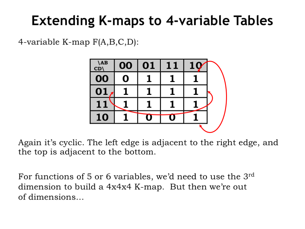
It’s easy to extend the K-map notation to truth tables for functions with 4 inputs, as shown here. We’ve used a Gray code sequencing for the rows as well as the columns. As before, the leftmost and rightmost columns are adjacent, as are the top and bottom rows. Again, as we move to an adjacent column or an adjacent row, only one of the four input labels will have changed.
To build a K-map for functions of 6 variables we’d need a 4x4x4 matrix of values. That’s hard to draw on the 2D page and it would be a challenge to tell which cells in the 3D matrix were adjacent. For more than 6 variables we’d need additional dimensions. Something we can handle with computers, but hard those of us who live in only a three-dimensional space!
As a practical matter, K-maps work well for up to 4 variables, and we’ll stick with that. But keep in mind that you can generalize the K-map technique to higher dimensions.
So why talk about K-maps? Because patterns of adjacent K-map entries that contain 1’s will reveal opportunities for using simpler product terms in our sum-of-products expression.
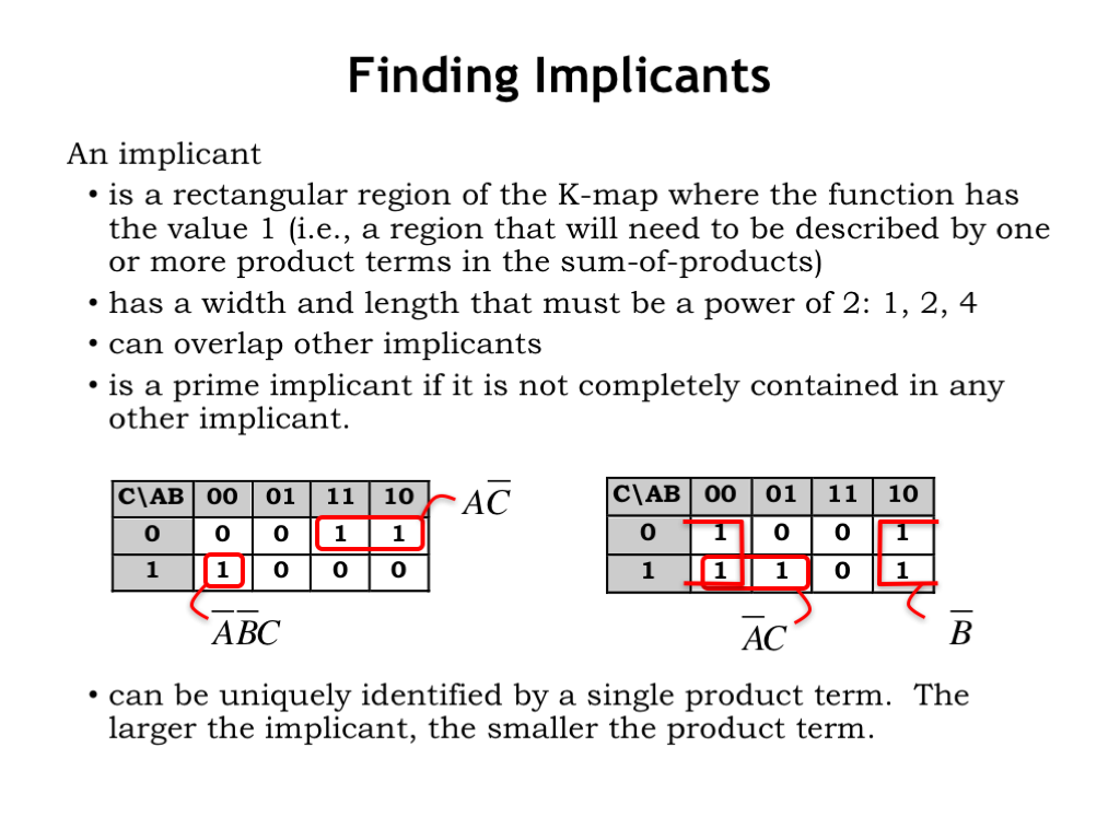
Let’s introduce the notion of an implicant, a fancy name for a rectangular region of the K-map where the entries are all 1’s. Remember when an entry is a 1, we’ll want the sum-of-products expression to evaluate to TRUE for that particular combination of input values.
We require the width and length of the implicant to be a power of 2, i.e., the region should have 1, 2, or 4 rows, and 1, 2, or 4 columns.
It’s okay for implicants to overlap. We say that an implicant is a prime implicant if it is not completely contained in any other implicant. Each product term in our final minimized sum-of-products expression will be related to some prime implicant in the K-map.
Let’s see how these rules work in practice using these two example K-maps. As we identify prime implicants, we’ll circle them in red. Starting with the K-map on the left, the first implicant contains the singleton 1-cell that’s not adjacent to any other cell containing 1’s.
The second prime implicant is the pair of adjacent 1’s in the upper right hand corner of the K-map. This implicant is has one row and two columns, meeting our constraints on an implicant’s dimensions.
Finding the prime implicants in the right-hand K-map is a bit trickier. Recalling that the left and right columns are adjacent, we can spot a 2x2 prime implicant. Note that this prime implicant contains many smaller 1x2, 2x1 and 1x1 implicants, but none of those would be prime implicants since they are completely contained in the 2x2 implicant.
It’s tempting draw a 1x1 implicant around the remaining 1, but actually we want to find the largest implicant that contains this particular cell. In this case, that’s the 1x2 prime implicant shown here. Why do we want to find the largest possible prime implicants? We’ll answer that question in a minute…
Each implicant can be uniquely identified by a product term, a Boolean expression that evaluates to TRUE for every cell contained within the implicant and FALSE for all other cells. Just as we did for the truth table rows at the beginning of this chapter, we can use the row and column labels to help us build the correct product term.
The first implicant we circled corresponds to the product term \(\overline{A} \cdot \overline{B} \cdot C\), an expression that evaluates to TRUE when A is 0, B is 0, and C is 1.
How about the 1x2 implicant in the upper-right hand corner? We don’t want include the input variables that change as we move around in the implicant. In this case the two input values that remain constant are C (which has the value 0) and A (which has the value 1), so the corresponding product term is \(A \cdot \overline{C}\).
Here are the two product terms for the two prime implicants in the right-hand K-map. Notice that the larger the prime implicant, the smaller the product term! That makes sense: as we move around inside a large implicant, the number of inputs that remain constant across the entire implicant is smaller. Now we see why we want to find the largest possible prime implicants: they give us the smallest product terms!
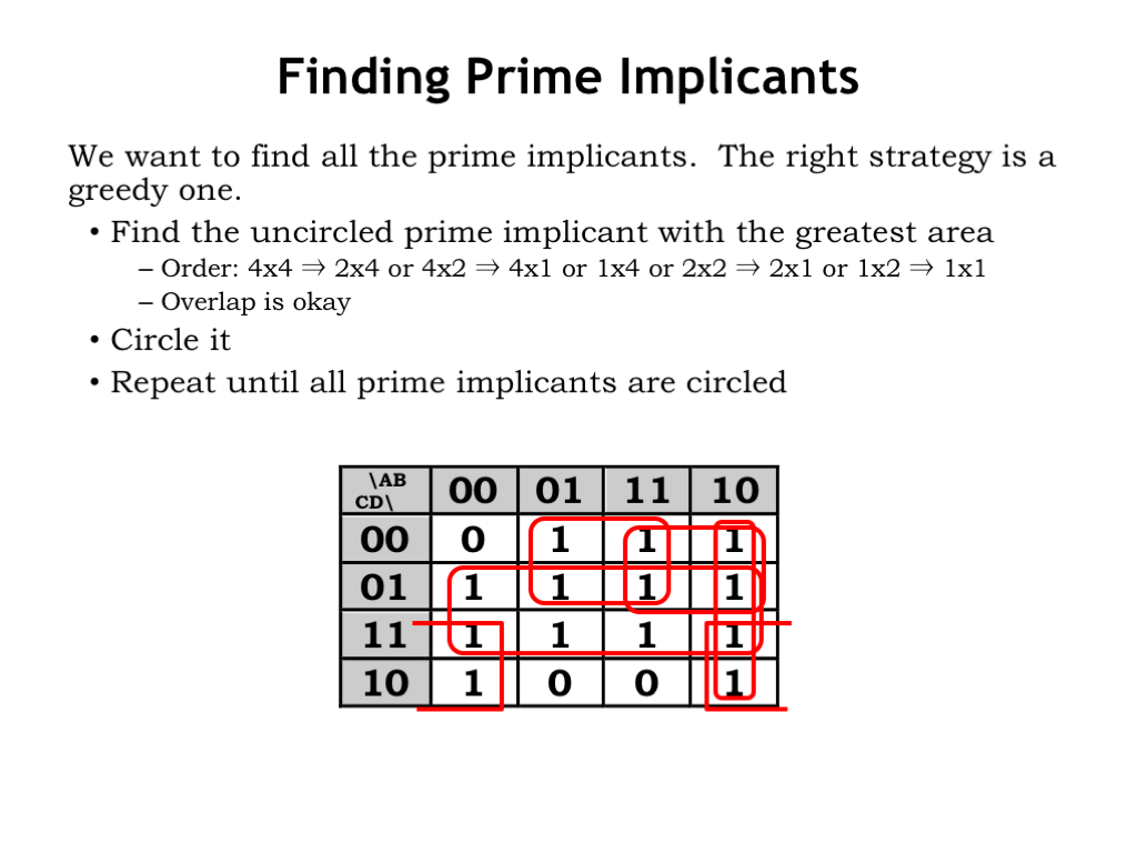
Let’s try another example. Remember that we’re looking for the largest possible prime implicants. A good way to proceed is to find some un-circled 1, and then identify the largest implicant we can find that incorporates that cell.
There’s a 2x4 implicant that covers the middle two rows of the table. Looking at the 1’s in the top row, we can identify two 2x2 implicants that include those cells.
There’s a 4x1 implicant that covers the right column, leaving the lonely 1 in the lower left-hand corner of the table. Looking for adjacent 1’s and remembering the table is cyclic, we can find a 2x2 implicant that incorporates this last un-circled 1.
Notice that we’re always looking for the largest possible implicant, subject to constraint that each dimension has to be either 1, 2 or 4. It’s these largest implicants that will turn out to be prime implicants.
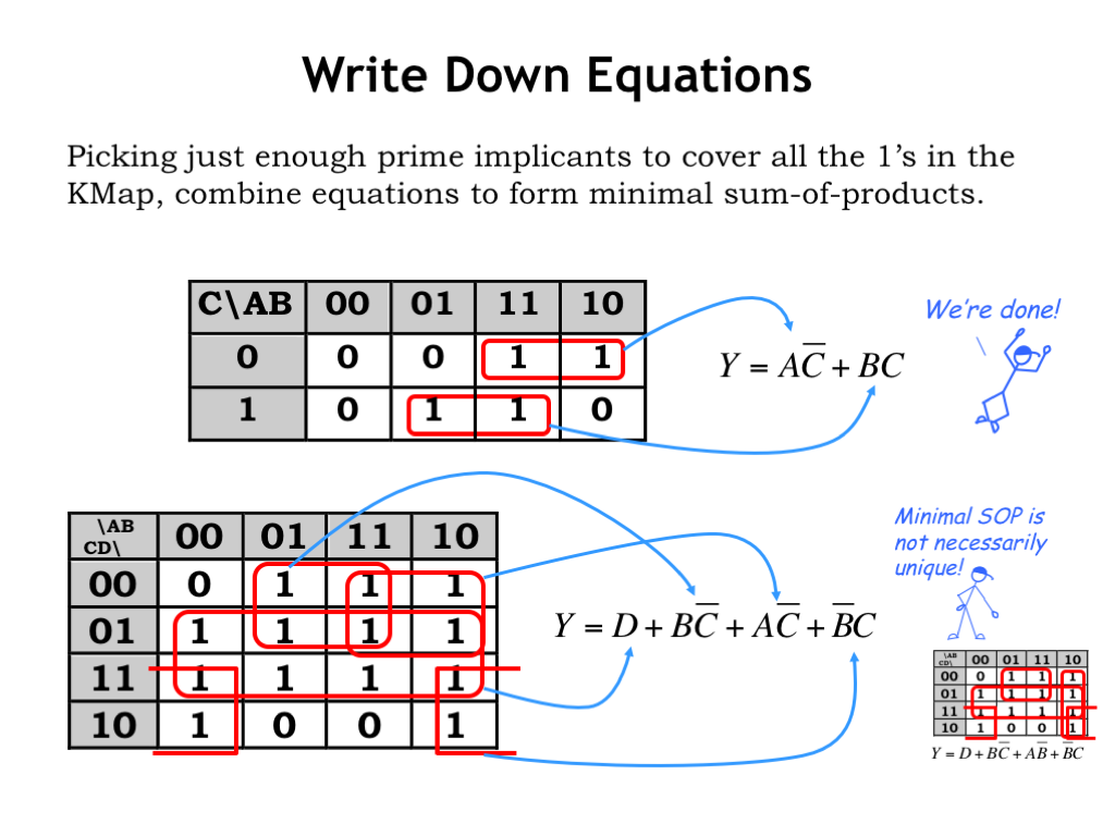
Now that we’ve identified the prime implicants, we’re ready to build the minimal sum-of-products expression.
Here are two example K-maps where we’ve shown only the prime implicants needed to cover all the 1’s in the map. This means, for example, that in the 4-variable map, we didn’t include the 4x1 implicant covering the right column. That implicant was a prime implicant since it wasn’t completely contained by any other implicant, but it wasn’t needed to provide a cover for all the ones in the table.
Looking at the top table, we’ll assemble the minimal sum-of-products expression by including the product terms for each of the shown implicants. The top implicant has the product term A AND (not C), and the bottom implicant has the product term (B AND C). And we’re done! Why is the resulting equation minimal? If there was some further reduction that could be applied, to produce a yet smaller product term, that would mean there was a larger prime implicant that could have been circled in the K-map.
Looking the bottom table, we can assemble the sum-of-products expression term-by-term. There were 4 prime implicants, so there are 4 product terms in the expression.
And we’re done. Finding prime implicants in a K-map is faster and less error-prone that fooling around with Boolean algebra identities.
Note that the minimal sum-of-products expression isn’t necessarily unique. If we had used a different mix of the prime implicants when building our cover, we would have come up with different sum-of-products expression. Of course, the two expressions are equivalent in the sense that they produce the same value of Y for any particular combination of input values — they were built from the same truth table after all. And the two expressions will have the same number of operations.
So when you need to come with up a minimal sum-of-products expression for functions of up to 4 variables, K-maps are the way to go!
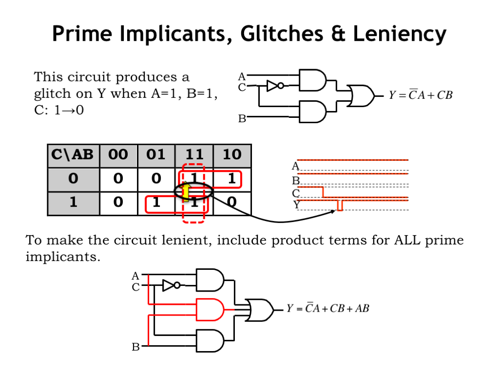
We can also use K-maps to help us remove glitches from output signals. Earlier in the chapter we saw this circuit and observed that when A was 1 and B was 1, then a 1-to-0 transition on C might produce a glitch on the Y output as the bottom product term turned off and the top product term turned on.
That particular situation is shown by the yellow arrow on the K-map, where we’re transitioning from the cell on the bottom row of the 1-1 column to the cell on the top row. It’s easy to see that we’re leaving one implicant and moving to another. It’s the gap between the two implicants that leads to the potential glitch on Y.
It turns out there’s a prime implicant that covers the cells involved in this transition shown here with a dotted red outline. We didn’t include it when building the original sum-of-products implementation since the other two product terms provided the necessary functionality. But if we do include that implicant as a third product term in the sum-of products, no glitch can occur on the Y output.
To make an implementation lenient, simply include all the prime implicants in the sum-of-products expression. That will bridge the gaps between product terms that lead to potential output glitches.
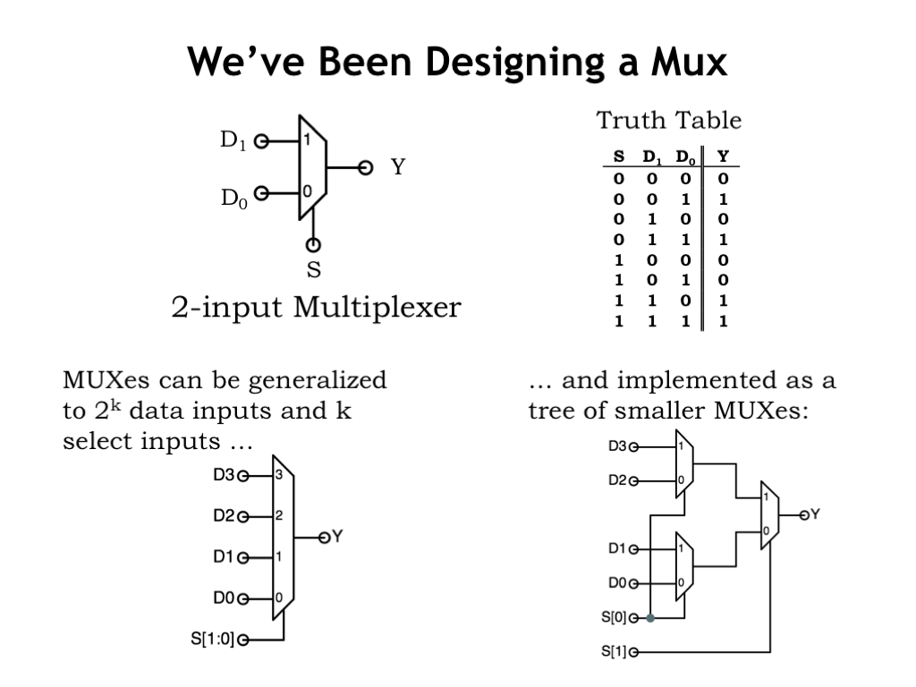
The truth table we’ve been using as an example describes a very useful combinational device called a 2-to-1 multiplexer. A multiplexer, or MUX for short, selects one of its two input values as the output value. When the select input, marked with an S in the diagram, is 0, the value on data input D0 becomes the value of the Y output. When S is 1, the value of data input D1 is selected as the Y output value.
MUXes come in many sizes, depending on the number of select inputs. A MUX with K select inputs will choose between the values of \(2^K\) data inputs. For example, here’s a 4-to-1 multiplexer with 4 data inputs and 2 select inputs.
Larger MUXes can be built from a tree of 2-to-1 MUXes, as shown here.
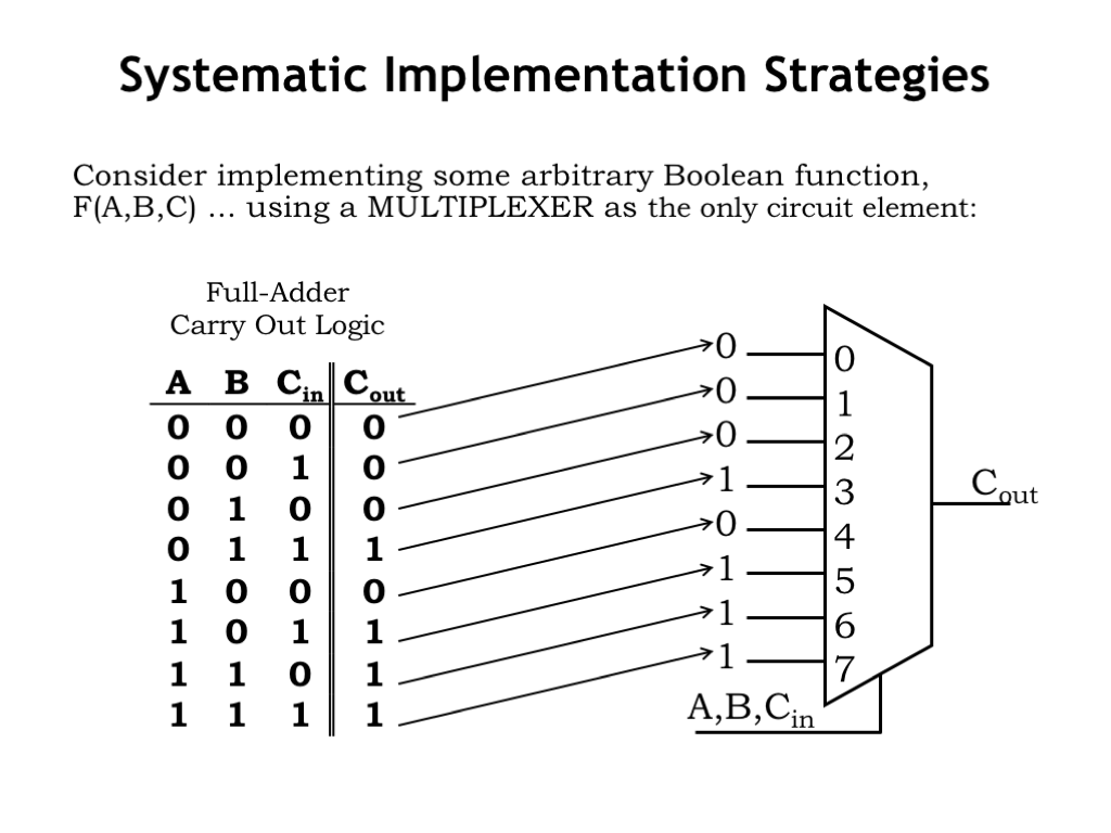
Why are MUXes interesting? One answer is that they provide a very elegant and general way of implementing a logic function. Consider the 8-to-1 MUX shown on the right. The 3 inputs — A, B, and CIN — are used as the three select signals for the MUX. Think of the three inputs as forming a 3-bit binary number. For example, when they’re all 0, the MUX will select data input 0, and when they’re all 1, the MUX will select data input 7, and so on.
How does make it easy to implement the logic function shown in the truth table? Well, we’ll wire up the data inputs of the MUX to the constant values shown in the output column in the truth table. The values on the A, B and CIN inputs will cause the MUX to select the appropriate constant on the data inputs as the value for the COUT output.
If later on we change the truth table, we don’t have to redesign some complicated sum-of-products circuit, we simply have to change the constants on the data inputs. Think of the MUX as a table-lookup device that can be reprogrammed to implement, in this case, any three-input equation. This sort of circuit can be used to create various forms of programmable logic, where the functionality of the integrated circuit isn’t determined at the time of manufacture, but is set during a programming step performed by the user at some later time. Modern programmable logic circuits can be programmed to replace millions of logic gates. Very handy for prototyping digital systems before committing to the expense of a custom integrated circuit implementation.
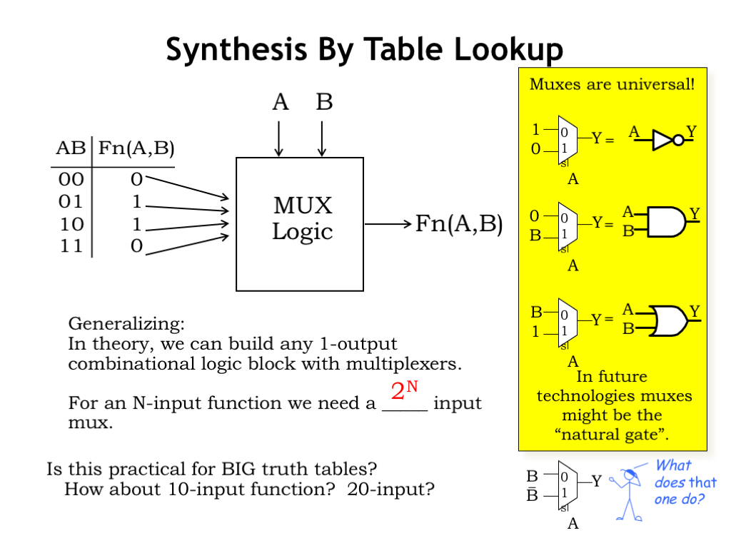
So MUXes with N select lines are effectively stand-ins for N-input logic circuits. Such a MUX would have \(2^N\) data inputs. They’re useful for N up to 5 or 6, but for functions with more inputs, the exponential growth in circuit size makes them impractical.
Not surprisingly, MUXes are universal as shown by these MUX-based implementations for the sum-of-products building blocks. There is some speculation that in molecular-scale logic technologies, MUXes may be the natural gate, so it’s good to know they can be used to implement any logic function.
Even XOR is simple to implement with a single 2-to-1 MUX!
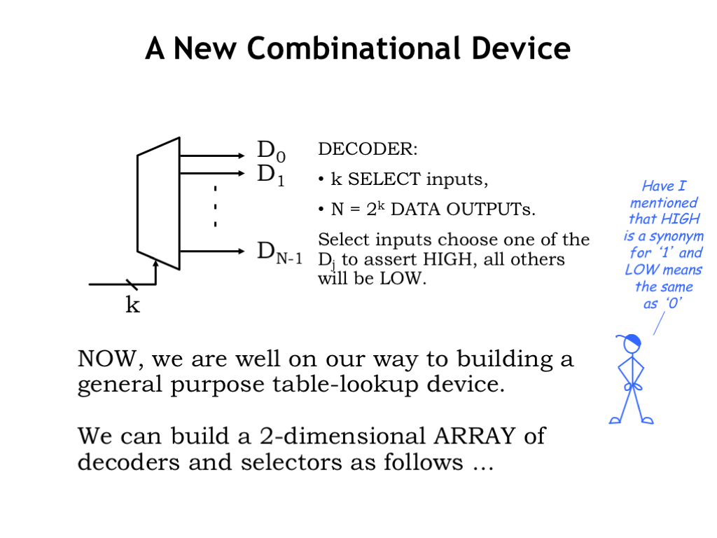
Here’s a final logic implementation strategy using read-only memories. This strategy is useful when you need to generate many different outputs from the same set of inputs, a situation we’ll see a lot when we get to finite state machines later on in the course. Where MUXes are good for implementing truth tables with one output column, read-only memories are good for implementing truth tables with many output columns.
One of the key components in a read-only memory is the decoder which has K select inputs and \(2^K\) data outputs. Only one of the data outputs will be 1 (or HIGH) at any given time, which one is determined by the value on the select inputs. The Jth output will be 1 when the select lines are set to the binary representation of J.
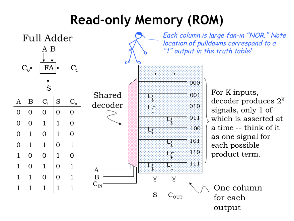
Here’s a read-only memory implementation for the 2-output truth table shown on the left. This particular 2-output device is a full adder, which is used as a building block in addition circuits.
The three inputs to the function (A, B, and CI) are connected to the select lines of a 3-to-8 decoder. The 8 outputs of the decoder run horizontally in the schematic diagram and each is labeled with the input values for which that output will be HIGH. So when the inputs are 000, the top decoder output will be HIGH and all the other decoder outputs LOW. When the inputs are 001 — i.e., when A and B are 0 and CI is 1 — the second decoder output will be HIGH. And so on.
The decoder outputs control a matrix of NFET pulldown switches. The matrix has one vertical column for each output of the truth table. Each switch connects a particular vertical column to ground, forcing it to a LOW value when the switch is on. The column circuitry is designed so that if no pulldown switches force its value to 0, its value will be a 1. The value on each of the vertical columns is inverted to produce the final output values.
So how do we use all this circuitry to implement the function described by the truth table? For any particular combination of input values, exactly one of the decoder outputs will be HIGH, all the others will be low. Think of the decoder outputs as indicating which row of the truth table has been selected by the input values. All of the pulldown switches controlled by the HIGH decoder output will be turned ON, forcing the vertical column to which they connect LOW.
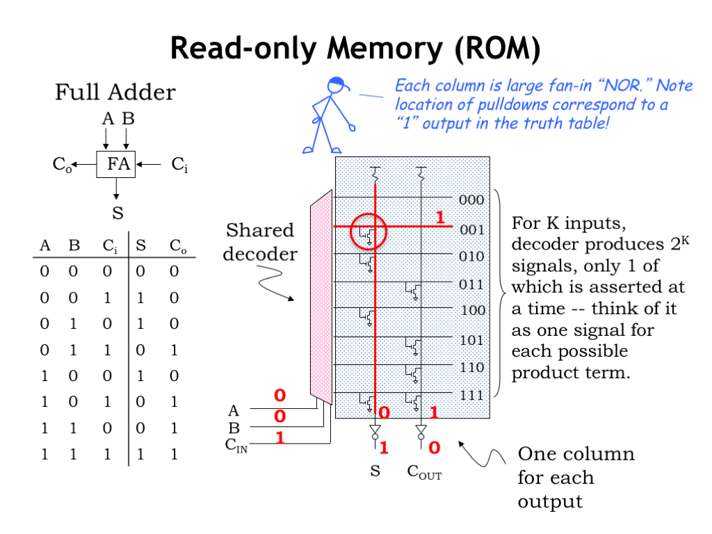
For example, if the inputs are 001, the decoder output labeled 001 will be HIGH. This will turn on the circled pulldown switch, forcing the S vertical column LOW . The COUT vertical column is not pulled down, so it will be HIGH. After the output inverters, S will be 1 and COUT will be 0, the desired output values.
By changing the locations of the pulldown switches, this read-only memory can be programmed to implement any 3-input, 2-output function.
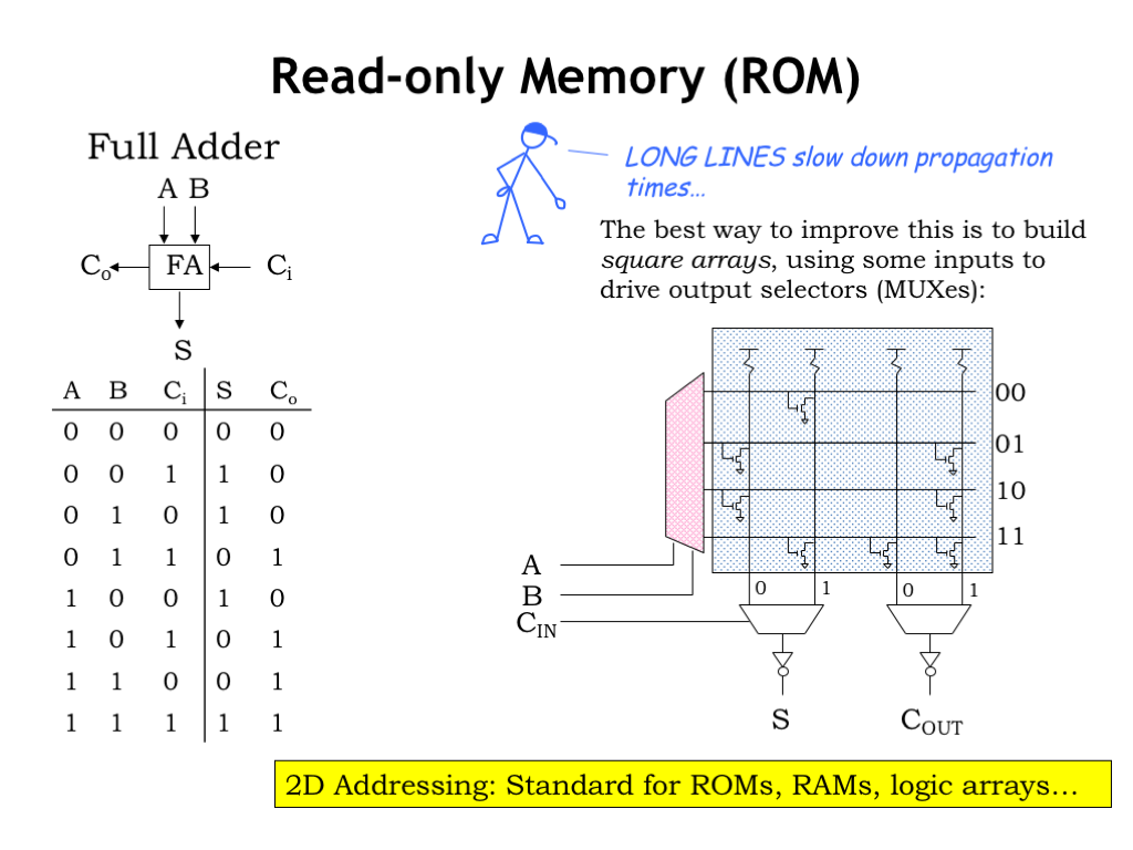
For read-only memories with many inputs, the decoders have many outputs and the vertical columns in the switch matrix can become quite long and slow. We can reconfigure the circuit slightly so that some of the inputs control the decoder and the other inputs are used to select among multiple shorter and faster vertical columns. This combination of smaller decoders and output MUXes is quite common in these sorts of memory circuits.
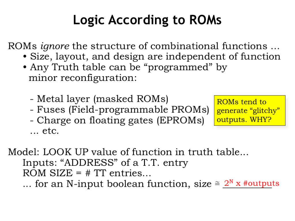
Read-only memories, ROMs for short, are an implementation strategy that ignores the structure of the particular Boolean expression to be implemented. The ROM’s size and overall layout are determined only by the number of inputs and outputs. Typically the switch matrix is fully populated, with all possible switch locations filled with an NFET pulldown. A separate physical or electrical programming operation determines which switches are actually controlled by the decoder lines. The other switches are configured to be in the permanently off state.
If the ROM has N inputs and M outputs, then the switch matrix will have \(2^N\) rows and M output columns, corresponding exactly to the size of the truth table.
As the inputs to the ROM change, various decoder outputs will turn off and on, but at slightly different times. As the decoder lines cycle, the output values may change several times until the final configuration of the pulldown switches is stable. So ROMs are not lenient and the outputs may show the glitchy behavior discussed earlier.
Whew! This has been a whirlwind tour of various circuits we can use to implement logic functions. The sum-of-products approach lends itself nicely to implementation with inverting logic. Each circuit is custom-designed to implement a particular function and as such can be made both fast and small. The design and manufacturing expense of creating such circuits is worthwhile when you need high-end performance or are producing millions of devices.
MUX and ROM circuit implementations are mostly independent of the specific function to be implemented. That’s determined by a separate programming step, which may be completed after the manufacture of the devices. They are particularly suited for prototyping, low-volume production, or devices where the functionality may need to be updated after the device is out in the field.


